🔬 Lab 1: VGA Synchronization#
📌 Objectives#
Students should be able to generate a time-critical signal, VGA.
📜 Synopsis#
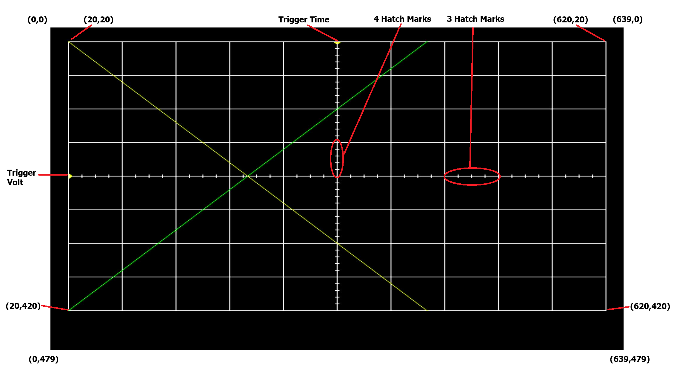
In this lab, you will write a VGA controller in VHDL and implement it on your FPGA development board. You will be provided a VGA-to-HDMI module that will automatically format your output for the HDMI output port on your development board. This VGA controller will be tasked to generate the display portion of an oscilloscope as shown in the figure below. The scope face consists of a white grid, used to measure the signals, two trigger markers, and the waveforms. The grid shall contain 11 vertical lines and 9 horizontal lines. In this lab, the waveforms (diagonal lines) will be artificially generated by your code, but in later labs, the waveforms will be generated by incoming audio waveforms.
🧮 Procedure#
💻 VGA Overview#
Video Graphics Array (VGA) is an interface protocol used to transmit analog video data to a screen. The VGA protocol uses a scanning method to project an image on the screen. Starting in the top-left of the screen, the monitor will progressively move from left to right, top to bottom to display each pixel. The following signals must be sent to a VGA monitor in order to display an image.
red,green,blue- three separate analog voltage signals indicating the amount of each color to display in the current pixel. These signals are sometimes abbreviated as RGB.h_sync- Horizontal synchronization signal that tells the screen to start writing pixels to the next linev_sync- Vertical synchronization signal that tells the screen that the current video frame is completed. The screen then starts writing pixels to the top-left of the screen.
Both synchronization signals contain four unique states: active_video, front_porch, sync_pulse, and back_porch. Incoming pixel data (through the RGB channels) is only displayed during the active_video state of the synchronization signals.
Internally, you will use a 25MHz clock as your pixel_clk. On the rising edge of this clock, when both the h_sync and v_sync signals are in the active_video state, you will place the RGB values you want the screen to display for that pixel. During all other states, the RGB values must be “0”.
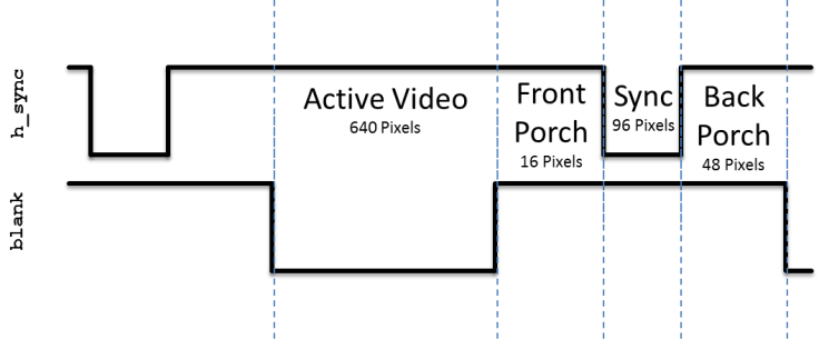
Figure 1: The h_sync signal contains four states. Pixel data is only displayed on the monitor during the active_video state. During all other state, the RGB values must be “0”.
The v_sync signal looks nearly identical to the h_sync signal, however it is significantly stretched out in time. Where the h_sync signal was counted in terms of pixel_clk, the v_sync signal is counted based on iterations of the h_sync signal. For example, in Figure 2, the active_video portion is active for 480 complete iterations of the h_sync signal.
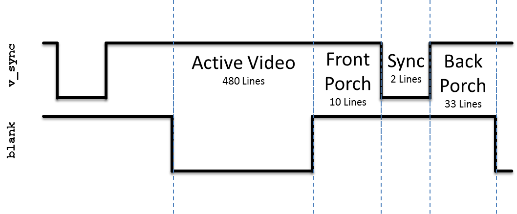
Figure 2: The v_sync signal is similar to h_sync, but instead of counting based on pixel_clk, the states are based on the number of iterations of the h_sync signal. Pixel data is only displayed on the monitor during the active_video state. During all other state, the RGB values must be “0”.
More details on the VGA protocol can be found at http://www-mtl.mit.edu/Courses/6.111/labkit/vga.shtml. This link provides the exact numbers needed to generate the correct timing pulse signals for any VGA resolution. And this youtube video illustrates how the old CRT works: How a TV Works in Slow Motion - The Slow Mo Guys .
VHDL Code#
In order to get you going in this lab, some of the VHDL code has been provided for you. In most cases, you should refrain from changing the modules given. In order to get a better understanding how these modules interact with one another, the following sections provide a schematic and the input, output and behavior of some of the modules.
lab1.vhdl
video.vhdl
numeric_stepper.vhd
numeric_stepper_tb.vhd
dvid.vhdl
tdms.vhdl
vga.vhd
vga_signal_generator.vhd
color_mapper.vhd
ece383_pkg.vhd
All of this code is in this ZIP file: Lab1_Cadet_Code_2026.zip
Project Setup#
Architecture#
The design of Lab 1 is broken down into separate components, some of which are provided for you and some which you will need to create. The interconnection of the components is illustrated in the following schematic. When a signal name appears just inside a box, that should should correspond to the name of that signal in the entity description. Please note there are a few omissions in the diagram that you should correct as part of your documentation (see Turn-In section).
Before reading about each component it’s recommended to review the ece383_pkg package to get familiar with the subtypes, record types, functions, and component declarations as these are used throughout the project.
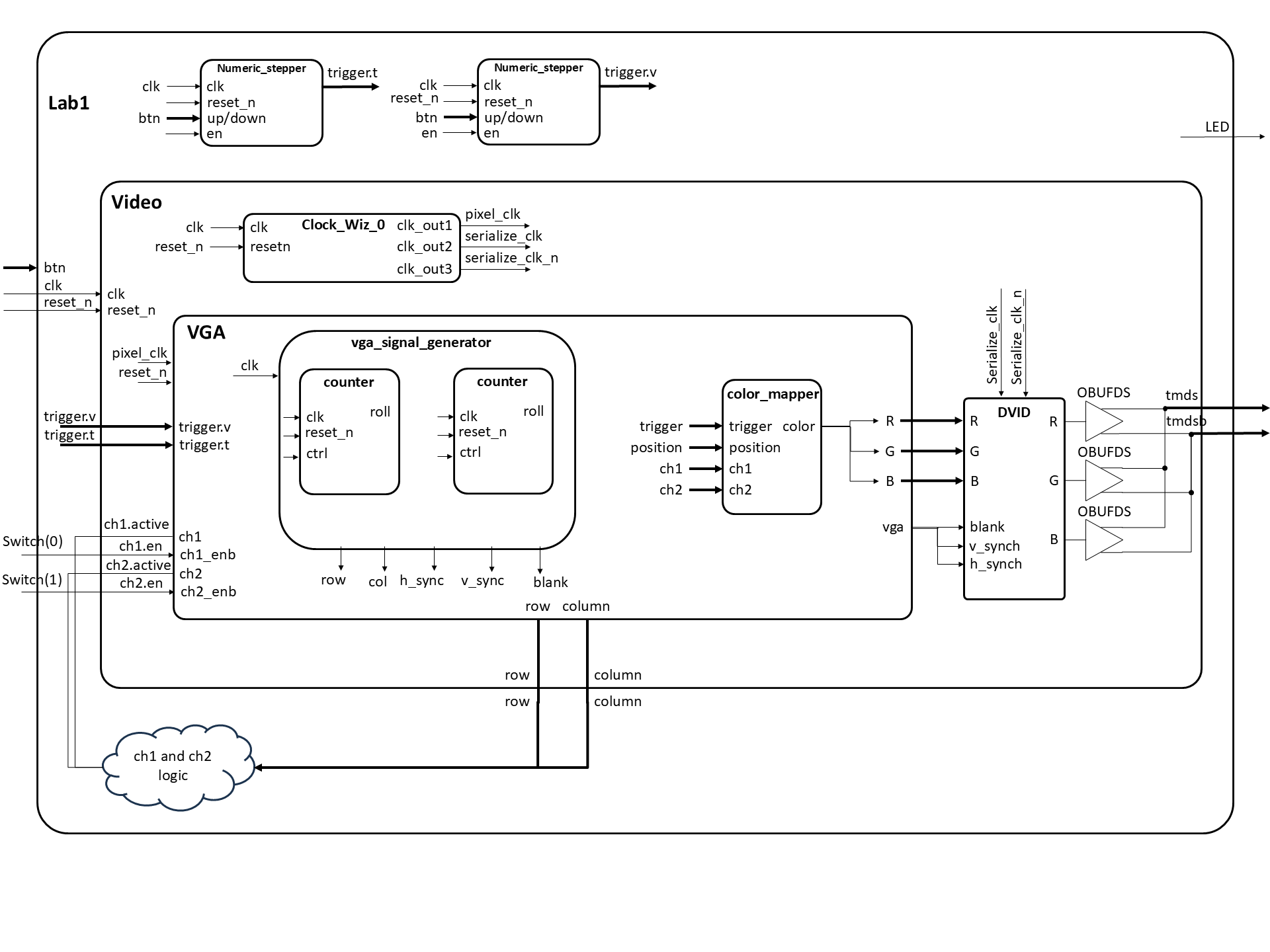
There are two components which will constitute the majority of your work, vga_signal_generator and color_mapper. The following two subsections detail the behavior of these two modules.
The vga_signal_generator component#
Your main task is to build the vga_signal_generator component for Lab1. This component sweeps across the display from left to right, and then returns to the left side of the next lower row. The VGA interface determines the color of each pixel on this journey with the help of the color_mapper component.
entity vga_signal_generator is
    Port ( clk : in STD_LOGIC;
           reset_n : in STD_LOGIC;
           position: out coordinate_t;
           vga : out vga_t);
end vga_signal_generator;
Signal |
Description |
|---|---|
|
This is the 25MHz pixel clock generated by the DCM in the video module. |
|
This is the same active high reset signal passed into the top level Lab1 module. |
|
This is a record of coordinate_t type which holds the current pixel row and col from your counters |
|
This is a record of vga_t type which holds the hsync, vsync, and blank signals |
The color_mapper component#
Inside the VGA module sits an instance of the color_mapper component. This component only contains combinational logic. When given a row,column pair, its responsible for generating the R,G,B value of that pixel.
entity color_mapper is
    Port ( color : out color_t;
           position: in coordinate_t;
		   trigger : in trigger_t;
           ch1 : in channel_t;
           ch2 : in channel_t);
end color_mapper;
Signal |
Description |
|---|---|
|
The 24-bit color value that the current row and column map to |
|
The current row being processed on the display. |
|
The current column being processed on the display. |
|
A 11-bit signed value representing the trigger voltage. This value is used to display a yellow arrow (Trigger Level Marker) on the vertical axis. |
|
A 11-bit signed value representing the trigger time. This value is used to display a yellow arrow (Trigger Time Marker) on the horizontal axis. |
|
A 1-bit signal indicating whether to draw the channel 1 signal on the scope for the current row, column pixel. When the value is 1, draw a yellow pixel; when 0, do not draw a pixel. |
|
A 1-bit signal enabling the channel 1 signal to be drawn. |
|
A 1-bit signal indicating whether to draw the channel 2 signal on the scope for the current row, column pixel. When the value is 1, draw a green pixel; when 0, do not draw a pixel. |
|
A 1-bit signal enabling the channel 2 signal to be drawn. |
Note
trigger.t and trigger.v are signed values, even though they should never be negative, because the numeric_stepper was designed to be general purpose and reusable. You’ll want to convert it back to an unsigned type to work with our other signals. Since trigger.t can go up to 600 we use 11 bits for the trigger. This is because 2^11=2048 which gives us 0 to 1023 on the positive side of the range. Keeping everything positive makes the conversions easier.
Verification#
You can verify your vga_signal_generator and color_mapper components using the two test benches provided.
Warning
Run both of these testbenches for at least 40 ms to ensure all signals get checked and enough frames are produced to see the results.
vga_signal_generator_tb#
The VGA_Signal_Generator testbench runs your signal generator and compares the actual output of your component with the desired spec. Your instructor will either provide this to you or make it available as a GradeScope autograder after you’ve completed Gate Check 1. If you run the test bench on your own, ensure you run it for at least 50 ms to ensure all tests complete.
vga_log_tb#
This testbench runs your vga_signal_generator along with the color_mapper and logs the VGA signals to a text file. After running the testbench you should have a log file named vga_log.txt in your project folder. This should be in [Project Path]\[Project Name].sim\sim_1\behav\xsim by default. It’s recommended to run for 40 ms or more to capture at least two frames. Once you have your log file, go to https://madlittlemods.github.io/vga-simulator/. Click Choose File and select your vga_log.txt file. The default settings of the simulator should be 640x480 @ 25MHz which is what we want. Click Submit and the simulator will start displaying the frames of the display output.
Testing#
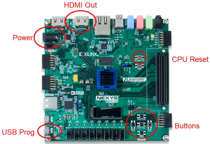
Your Digilent board will have a lot of connections required to make this lab work. The image below shows where these connections are made. You will need to setup your constraints file to connect the FPGA pins to your design.
🚚 Deliverables#
Gate Check 1#
[5 Points]
By end of day on Lesson 7, you must have finished setting up the VGA counters to generate the proper rows and columns on the waveform. This can be shown with waveform screenshots from the VGA testbench showing the h count rolling over causing the v count to increment. Be sure to also show both max counts. You must implement the two counters similar to the method implemented for the counters in Homework 4.
Show both the row and column max counts rolling over back to zero
Place all screenshots in a single document and upload it to GradeScope.
Push your code to your GitHub repository using git with the tag
Lab1_GC1
Gate Check 2#
[5 Points]
By end of day on Lesson 8, you must have setup the appropriate vsync, hsync, and blank signals on the waveform. You should also be at the point where you’ve created the color_mapper module to draw at least one line on the display, though this isn’t required for the turn-in.
Submit your vga_signal_generator.vhd and counter.vhd to GradeScope under LAB1_GC2_CODE
Push your code to your GitHub repository using git with the tag
Lab1_GC2
Required Functionality#
[35 Points]
For Required Functionality your code must generate the white oscilloscope grid pattern shown in the figure above and draw the two channels of traces. To test this draw:
The channel 1 trace (yellow) along a diagonal where (row = column).
The channel 2 trace (green) should be drawn along a diagonal where (row = 440-column).
Switch(0) should be able to enable and disable channel 1
Switch(1) should be able to enable and disable channel 2
This test code should be placed in the Lab1 entity.
You need to draw the channel 1 trace (yellow) along a diagonal where (row = column). The channel 2 trace (green) should be drawn along a diagonal where (row = 440-column). This test code should be placed in the Lab1 entity (not in color_mapper). This means you have some logic in the Lab1 entity that uses the column coming out of the Video component to provide an input row value for each channel.
Demo can be live to your instructor or a video uploaded to Teams.
Push your code to your repository using git with the tag
Lab1_ReqdFunc
A Functionality#
[15 Points]
Demo to the instructor your live program with the o’scope grid pattern generated on the monitor, ch1 with a yellow diagonal line and ch2 with a green diagonal line. Demo the ability to enable and disable ch1 and ch2 with switches. See figure above.
A-level functionality is shown in the figure in the Lab Overview section at the top of the page. In addition to drawing the display, the display must update when one of the buttons is pressed according to the list below.
Pressing the upper directional button (BTNU) once should move the Trigger Level Marker up.
Pressing the lower directional button (BTND) once should move the Trigger Level Marker down.
Pressing the left directional button (BTNL) once should move the Trigger Time Marker left.
Pressing the right directional button (BTNR) once should move the Trigger Time Marker right.
In order to achieve this level of functionality, you will need to implement the two numeric_stepper trigger components in the Lab1 schematic. These buttons do not need to be “debounced.” However, if you debounce your buttons properly you can earn 3 bonus points.
Demo can be live to your instructor or a video uploaded to Teams.
Push your code to your repository using git with the tag
Lab1_AFunc
README#
[25 Points]
All your work in this lab is to be uploaded to GitHub and you will tag the commits to record the time each milestone is completed. The main part of the lab is your README, documenting your design. The README should be in markdown in the Lab1 folder so it displays when viewing the folder on github.com.
Your README must include the following:
Introduction - Provide a brief overview of the problem.
Design/Implementation - Include your diagrams from HW5. Provide the block-diagram of your solution using the signal names in your code. The block diagram given above is somewhat incomplete, make sure to include corrections to this diagram. An editable block diagram PPT is provided here. For each component that you built, explain its overall purpose, inputs, outputs, and behavior. You do not need to include code in this report (instead put all your vhdl files (code and testbench), wcfg file, and bit files in GitHub). Tip: How to add images to your README
Test/Debug - Briefly describe the methods used to verify system functionality (such as products from gate check 1 and 2).
Show at least three excerpts from your testbench for the VGA module (as screen shots):
Show the hsync going high, low, and high in relation to column count.
Show the vsync going high, low, and high in relation to row count AND column count.
Show the blank signals going high, low, and high in relation to column count and row count.
Show the column count rolling over causing the row count to increment and max counts for both counters.
List the major problems you encountered and how you fixed them. This should cover all the problems you encountered in the lab and how you fixed them. Break each problem and solution into separate paragraphs.
Results - This section should clearly state for each milestone/functionality the date/time it was achieved, level of achievement (e.g, achieved, partially-achieved, not achieved), what was achieved, and evidence you proved it worked (e.g., via demo or images/videos). We no longer use the printed lab cutsheets signed by your instructor as you meet each milestone, but instead have you make a submission in Gradescope and Github for each milestone.
Conclusion - Explain what your learned from this lab and what changes you would recommend in future years to this lab or the lectures leading up to this lab.
Print your README.md to PDF then upload to GradeScope.
Coding Practices#
[5 Points] Use of Git and GitHub
[10 Points] Code style. Your code should be readable, concise, and well-organized. Points will be deducted for code that is difficult to understand and maintain. Write your code as if someone else is going to have to update it. The closer it is to plain english, the better.
Warning
Keep an eye on individual gate check turn in dates. The final turn in of all products (code, demos, and README) is end of day on Lesson 9.