🔬 Lab 2: Data Acquisition, Storage and Display#
📜 Lab Overview#
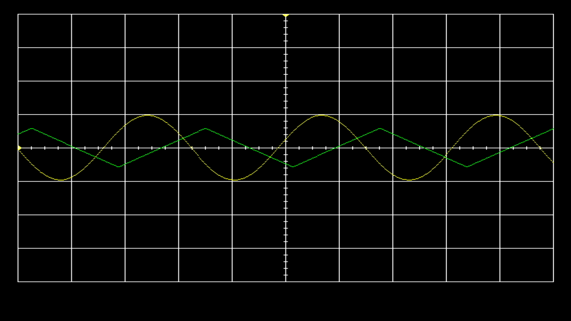
In this lab, we will integrate the video display controller developed in Lab 1 with the audio codec on the Nexys Video board to build a basic 2-channel oscilloscope. When complete, your lab should generate an output similar to the picture below.
💻 Procedure#
Architecture#
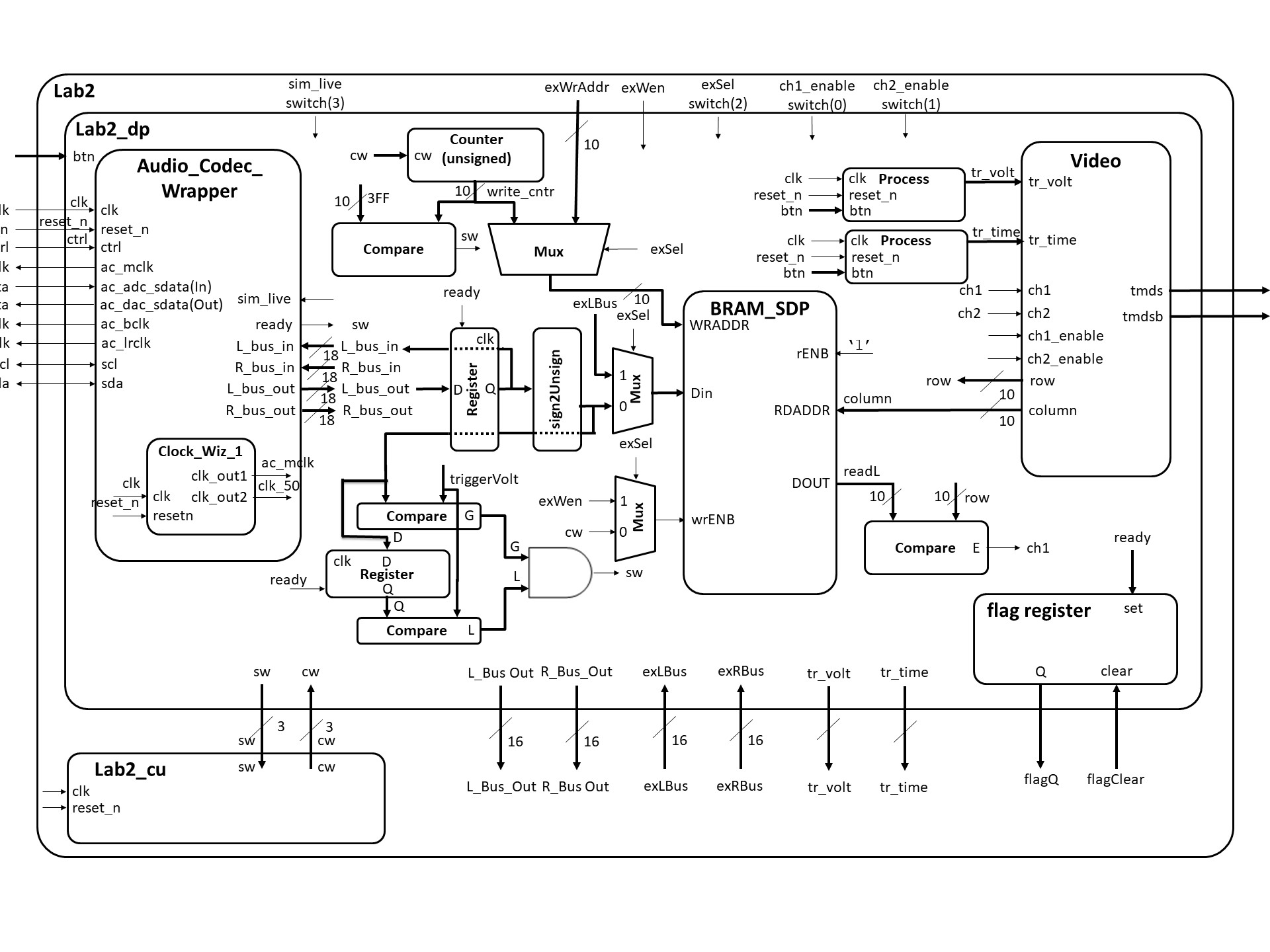
Just like the design of Lab 1, Lab 2 is broken down into a bunch of separate modules, shown in the block diagram below. Some of the components in the block diagram will be given to you and some you created in Lab 1. It is important to note that some of the components and signals associated with this diagram will not be needed for Lab 2, but have been included because you will need them in Labs 3 and 4.
Schematic Walk-through#
Consider the data in the diagram as flowing from left to right. You will provide an input signal to the Nexys board via a 3.5mm cable connected to the blue line-in jack. This signal then passes through an Analog Devices ADAU1761 SigmaDSP Audio Codec. The ADAU1761 samples the audio input at 48kHz into separate 18-bit 2’s complement left and right channels. The ADAU1761 then transfers this data to our Artix 7 chip over a serial bus through the 7 signals on the left side of the Lab 2 component. You can read more about the audio codec on page 27 of the Nexys Video manual.
The serial protocol coming from the audio codec is quite complex, so you will be given the Audio Codec Wrapper component as an interface to extract the incoming signal (Audio Codec Wrapper in the Figure above). Whenever new converted data is ready from the Audio Codec, the ready signal will go high for a single clock cycle. Your circuit will then do two things with the incoming L_bus_out and R_bus_out signals: First, it will loop both of these signals back into the Audio Codec so that you can verify (by listening on the green line-out jack) that the Audio Codec hardware and firmware are operating correctly. This is accomplished using the VHDL code below.
Loopback Code Example#
Below is an example of looping back the audio signals in VHDL:
process (clk)
begin
    if (rising_edge(clk)) then
        if reset_n = '0' then
            L_bus_in <= (others => '0');
            R_bus_in <= (others => '0');
        elsif (ready = '1') then
            L_bus_in <= L_bus_out;
            R_bus_in <= R_bus_out;
        end if;
    end if;
end process;
Second, your circuit will need to send the L_bus_out and R_bus_out signals in an unsigned format to be stored in the block ram (BRAM). To do this, you will need to convert the 2’s complement values to unsigned. Performing this conversion is technically easy, but may be a little difficult to wrap your head around, so let’s do some examples. Consider the table below.
Two’s Complement to Unsigned Conversion#
The values in the left two columns represent the 2’s complement number coming out of the Audio Codec, while the right two columns represent the output of the “sign2unsign” conversion.
2’s Complement |
Value |
Unsigned |
Value |
|---|---|---|---|
100…000 |
-131072 |
000…000 |
0 |
111…111 |
-1 |
011…111 |
131071 |
000…000 |
0 |
100…000 |
131072 |
000…001 |
1 |
100…001 |
131073 |
011…111 |
131071 |
111…111 |
262143 |
The values in the left 2 columns represent the 2’s complement number coming out of the Audio Codec, in this case L_bus_out, while the right 2 columns represent the output of the box labeled “sign2unsign” in the block diagram. What we are essentially doing is shifting the unsigned values up by 131072 (the value which will make all 18-bit numbers positive) so that they all fall into a positive range. If you notice the pattern for these 5 number conversions, the lower 17-bits do not change. Only the most-significant-bit changes, and it is just inverted. In the zip file, there is a simple testbench called convert_unsigned_tb.vhdl you can modify to test this math. If you want to “not” the MSB and then concatenate “&” back the lower 17-bits, I’d recommend doing this as a std_logic_vector. You can also do this conversion with the number stored as an unsigned. In this case you can add a special number that keeps the lower 17-bits the same, but inverts the MSB. If you do this conversion correctly using the testbench, you should get an output simulation plot similar to sim_plot_test_convert.jpg in the zip file.
Here are a couple more pieces of info to help you understand the block diagram above. Consider the mux with its input going to the WRADDR input of the “BRAM_SDP” block in the block diagram. This mux circuitry attached to the write address of the BRAM will be used in Lab3, allowing the microBlaze processor to take over write duties for the RAM (as opposed to an external signal from the Audio Codec). Independent of the write circuitry, the read circuit pulls data from the RAM, and draws the waveform. Unlike for the write circuitry, the read circuitry requires no FSM control.
Datapath Entity#
Since its a very complex piece of circuitry, the entity for the datapath (LAB2_DP in the block diagram) is given below.
entity lab2_datapath is
    Port(
        clk : in  STD_LOGIC;
        reset_n : in  STD_LOGIC;
        ac_mclk : out STD_LOGIC;
        ac_adc_sdata : in STD_LOGIC;
        ac_dac_sdata : out STD_LOGIC;
        ac_bclk : out STD_LOGIC;
        ac_lrclk : out STD_LOGIC;
        scl : inout STD_LOGIC;
        sda : inout STD_LOGIC;
        tmds : out  STD_LOGIC_VECTOR (3 downto 0);
        tmdsb : out  STD_LOGIC_VECTOR (3 downto 0);
        sw: out std_logic_vector(2 downto 0);
        cw: in std_logic_vector (2 downto 0);
        btn: in STD_LOGIC_VECTOR(4 downto 0);
        switch: in STD_LOGIC_VECTOR(3 downto 0);
        exWrAddr: in std_logic_vector(9 downto 0);
        exWen, exSel: in std_logic;
        Lbus_out, Rbus_out: out std_logic_vector(15 downto 0);
        exLbus, exRbus: in std_logic_vector(15 downto 0);
        flagQ: out std_logic;
        flagClear: in std_logic);
end lab2_datapath;
Flag Register#
In Lab 3, we will be integrating most of the components from this lab with the MicroBlaze processor (a processor we program onto our FPGA). In order to make this smooth, we will need a way to transfer information between the two systems a technique similar to a 2-line handshake. To make this possible, you will need to build a component called a flag register. The behavior of the flag register is shown in the table below.
clk |
reset_n |
set |
clear |
Q+ |
|---|---|---|---|---|
0,1,falling |
X |
X |
X |
Q |
rising |
0 |
X |
X |
0 |
rising |
1 |
0 |
0 |
Q |
rising |
1 |
1 |
0 |
1 |
rising |
1 |
0 |
1 |
0 |
rising |
1 |
1 |
1 |
X |
The 1-bit flag register will interface our lab2 component with a MicroBlaze in lab3 as follows: The LAB2 component will produce some data, put it on a data line to the MicroBlaze, and then set the flag register using the READY signal. Then, the MicroBlaze will, at some point, look at the flag register bit. When it sees that the ‘set’ bit is 1, the MicroBlaze will grab the data from the register and clear the set bit. These are just like the flag bits on the 382 ARM processor.
BRAM#
You need to map the ports of BRAM to include it in your lab2_datapath. The component is declared in the UNIMACRO library - look at the BRAM documentation from that library to figure out how to port map BRAM.
	library UNIMACRO;		-- This contains links to the Xilinx block RAM
	use UNIMACRO.vcomponents.all;
Switches#
Switch(0): ch1_enable
Switch(1): ch2_enable
Switch(2): ex_Sel / is_ex : ‘1’ when external control is selected
Switch(3): sim_live / is_live : ‘1’ when live data is selected
Connections#
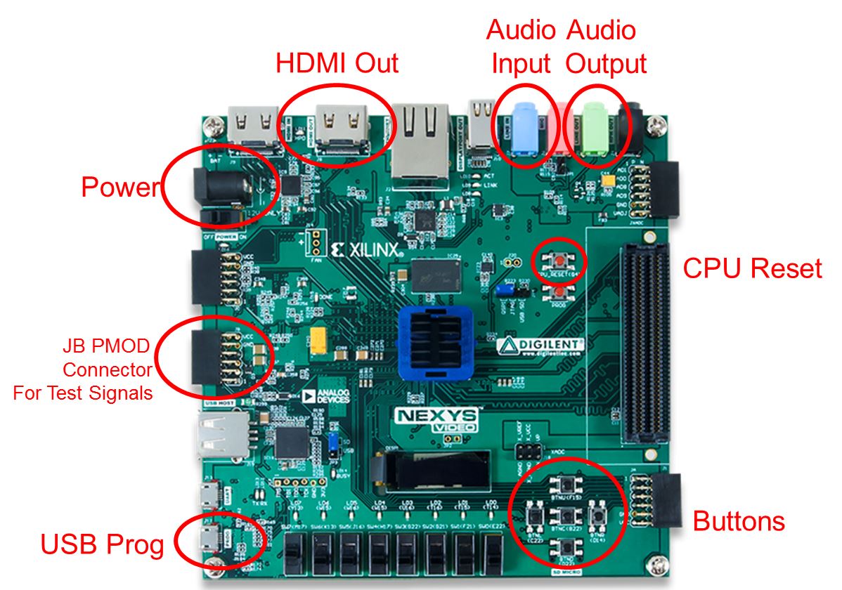
Generating Audio Waveforms#
Since you need to use a 3.5mm jack to input signals to the Nexys board, your computer’s audio output works quite well. You can use the embedded tone generator below or a third-party tone generator to create a test signal.
Lab Files#
Lab 2
Lab 2 Datapath
ece383_pkg (updated from Lab 1)
Audio Codec Wrapper
FSM Template
Constraint File
Optional OLED component you can place in your Lab2 Top Level Design to show your current configuration on the OLD Display.
Project Setup#
🚚 Deliverables#
Required Functionality#
The lab requires displaying a single channel waveform with reliable triggering at a fixed voltage level. The requirements include:
Centering the waveform on the grid (row 220)
Using separate datapath and control units
Implementing a flag register for communication with the MicroBlaze
Implementing BRAM initialization
Gate Checks#
There are 3 gate checks associated with this lab, each worth 5 points - see the rubric below. This year we will use Gradescope to track when you complete the milestones.
Gate Check 1#
[5 Points]
By end of day 1 (submit by day 2), you must have started a Lab 2 Vivado project and downloaded the template files and drop in your Video, VGA, Scopeface, dvid, and tdms files from Lab 1 into your Lab 2 project in order to test your Lab 1 color_mapper works when you implement your BRAM using the two initialized BRAM components given in lab2_datapath.vhdl. This does not require that the audio wrapper (and clockwiz_1) or your control unit is working yet, so you do not need to include these vhdl files in your design yet if you don’t want to. Your color_mapper/video should continuously be reading the left and right BRAM signals displaying them on the monitor. You must implement Video entity (from Lab 1) to take the channel output from the left and right BRAMs and send it to the Channel 1 and 2 inputs to be displayed when the readL and readR values equal the row value. Implement this on the hardware and verify that your scopeface is still present and some values are being displayed for Channel 1 (at this point the scaling may be wrong).
How do you read from BRAM continuously? From last lesson, to read we need to put the address we want to read on RDADDR, which in this case is the column requested by video; and when we enable the read RDEN, the BRAM will place the 16-bit data value at this address on DO. So to continually read, we set RDEN <= ‘1’. You can then compare this DO value with the current video’s row, and if they are equal, let ch1 <= ‘1’.
After you demo this, this is a good opportunity to work on scaling the signals so their DC value is centered on your grids y-axis. Note: the DC center value on your scope is row 220, while if you grabbed the upper ten bits from the BRAM DO, its DC center value will be 512 (a difference of del_x = 512-220 = 292). How does this change the comparator you use to assign ch1 and ch2? (which compares if ReadL = row… does it need to now compare something like if ReadL = row +/- del_x ?)
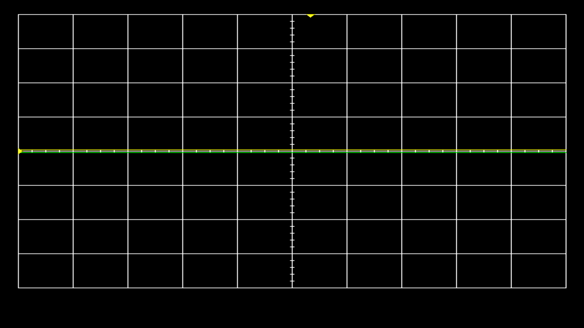
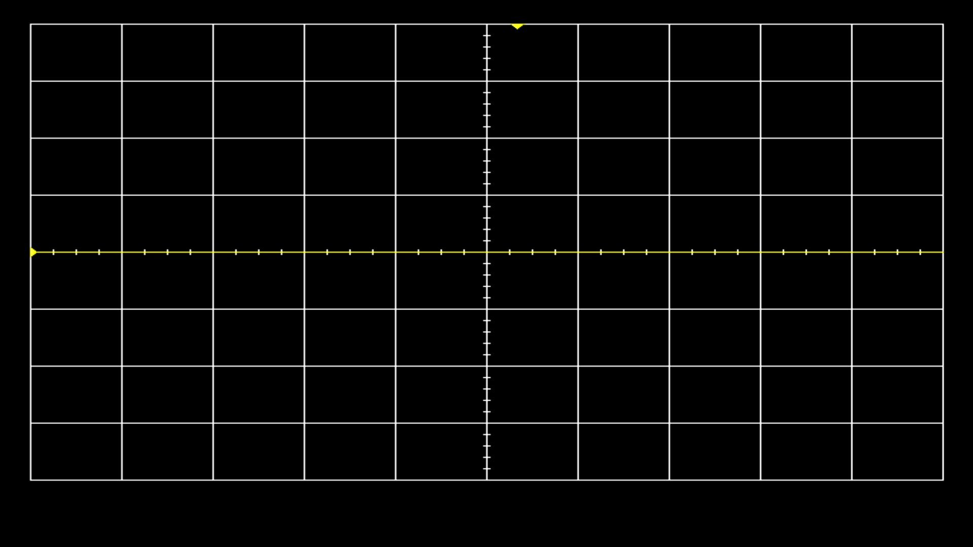
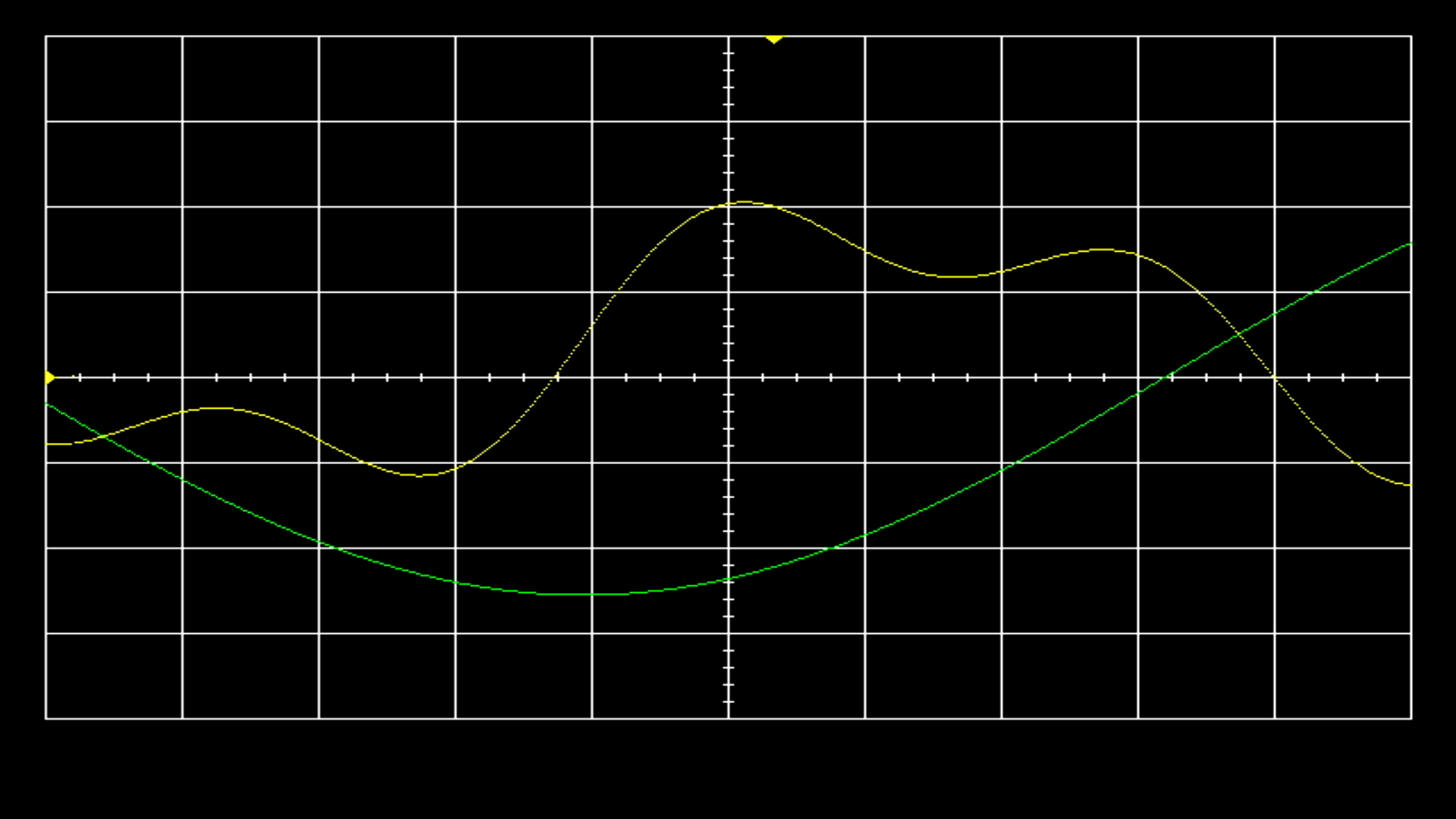
In the Lab2 Datapath there are comments that describe three tests you can do to progressively build towards displaying signals from the BRAM. Those tests should look like the following images.
Notice from the block diagram you will copy your Video instantiation and button processes from Lab 1 into your Lab 2 Datapath. You will also have to re-implement the Lab 1 Clocking Wizard in you Lab 2 project. Doing this will eliminate a lot of errors from un-driven output signals on lab 2 top. Additionally your color_mapper and Button inputs from Lab 1 should be functional as well. Also, you may need to implement another Clocking Wizard for the Audio Codec Wrapper inside the Datapath entity to get the bit stream to generate. The settings for the audio codec’s clock wizard are inside the audio codec files.
The demo can be live to your instructor or an image uploaded to teams.
Push your code to your GitHub repository using git with the tag
Lab2_GC1
Gate Check 2#
[5 Points]
NOTE: THIS IS THE HARDEST PART! By end of day 2 (submit by day 3), you must have implemented and connected the BRAM Address Counter to left and right BRAMs, instantiated the Audio Codec Wrapper in Simulation mode (sim_live = ‘0’), and your control unit, such that your control unit writes the simulated audio data to the left and right BRAM and you can see the waveforms plotted on the monitor. (at this point, since there is no trigger, the waveform may or may not be scrolling across the display and the scaling may be wrong. The simulated Audio Wrapper is continually sending out 1024 samples, and if your counter (with FSM) are in sync writing 1024 values, it will be writing the same 1024 values over and over, making the output waveforms on appear stationary. If you want the simulated waveforms to scroll as if they are not triggered, change your counter rollover to a lesser value like 640… remember there are only 640 columns on scopeface displayed. Another note about this counter: since your first column on your scopeface is column 20, should you initialize the counter at 20?).
How do you write a sample from the audio wrapper to the BRAM? From last lesson, to write we need to: (1) set WE => “11” [not using this feature], (2) put the address we want to write to on WRADDR, (3) put the converted data sample from the audio wrapper on the 16-bit data input DI, and (3) signal write enable WREN = ‘1’ with a CW from your FSM. Since the address we are writing to in the BRAM is controlled by the counter, your FSM needs to first reset the counter. Then it should wait for the Ready signal. When ready goes high, you can then save the sample (let WE = ‘1’ with a CW), then increment the counter (with a CW to increment the counter), then compare to see if you are done counting (by checking a SW). If not done counting, then jump back to wait for ready, otherwise, start the process over by jumping to the state to reset the counter.
Reminder: You must successfully convert the signed audio data from the Audio_Codec_Wrapper into unsigned data needed for the monitor. After you demo this, this is a good opportunity to work on scaling the signals so their DC value is centered on your grids y-axis and possibly work on the trigger hardware. If this does not work, you must create a Testbench to help debug why it is not working (see example testbenches in the zip file). Reminder: implement another Clocking Wizard and the Audio Codec Wrapper inside the Datapath entity to get your Audio Codec to begin functioning (if not done in gate check 1).
The demo can be live to your instructor or an image (if stationary) or video (if scrolling) uploaded to Teams.
Push your code to your GitHub repository using git with the tag
Lab2_GC2
Gate Check 3 - Implementing live audio input.#
[5 Points]
By end of day 3 (submit by day 4), redo Gate Check 2, except with the Audio Codec Wrapper in Live mode (sim_live / is_live = ‘1’). (at this point, since there is no trigger, the waveform will be scrolling across the display). Also make connections to loopback the serial ADC input back out to the DAC output (i.e. send the signal back into the Codec). Once you implement the design on the board, you can verify functionality by applying an audio signal to the audio line in jack (blue) and listening to it on the audio line out jack (Green), and seeing the output on the monitor. After you finish Gate Check 3, this is a good time to implement proper triggering on the trig_volt value. Besides the hardware to create the SW to signal the trigger, you’ll also need to add an initial state to “wait for trigger” in your FSM. The rest of the FSM is basically the same. If this does not work, you must create a Testbench to help debug why it is not working.
The demo can be live to your instructor or a video uploaded to Teams.
Required Functionality#
[30 Points]
Get a single channel of the oscilloscope to display with reliable triggering that holds the waveform at a single point on the left edge of the display (like having a fixed trigger_volt). A 220Hz waveform should display something similar to what is shown in the screenshot at the top of this page. Additionally, you must have the following done:
The waveform displayed should be centered about the center of the grid (row 220)
Use separate datapath and control unit.
The Mini-C design technique can be used but is NOT required. However, your instructor will expect you create Lab2_cu using the state machine coding style used in Lesson 9, with a process for state transitions, separated from a CSA LUT section for generating the output CWs.
Your datapath must use processes which are similar to our basic building block (counter, register, mux, etc.). I do not want to see one massive process that attempts to do all the work in the datapath.
The demo can be live to your instructor or a video uploaded to Teams.
Push your code to your GitHub repository using git with the tag
Lab2_ReqdFunc
B-level Functionality#
[10 Points]
You can swap the A and B functionality order if you’d like.
Meet all the requirements of required functionality.
Add a second channel (in green).
Include the flag register and exSel (and other ex___ signals) with their muxes as shown in the block diagram.
The demo can be live to your instructor or a video uploaded to Teams.
Push your code to your GitHub repository using git with the tag
Lab2_BFunc
A-level Functionality#
[10 Points]
Meet all the requirements of B-level functionality.
Use the trigger voltage marker to establish the actual trigger voltage used to capture the waveform. As the trigger is moved up and down, you should see the point at which the waveform intersects the left side of the screen change. The trigger arrow marker must be calibrated with the start of the waveform at column 20.
Integrate the button debouncing strategy in HW #7 (or an equivalent debouncing method) to debounce the buttons controlling the trigger time and trigger voltage.
Move the trigger volt and trigger time cursors on the screen using the buttons.
The demo can be live to your instructor or a video uploaded to Teams.
Push your code to your GitHub repository using git with the tag
Lab2_AFunc
Turn In#
All of your work in this lab is to be submitted using Github and you will make submission in Gradescope to record the time each milestone is completed.
README#
[20 Points]
The main part of the lab is your README, documenting your design. The README should be in markdown and should be uploaded to GitHub. Your README must include the following:
Introduction - Provide a brief overview of the problem.
Design/Implementation - Provide block-diagram of your solution using the signal names in your code. The block diagram given above is somewhat incomplete, so make sure to include corrections to it. Also, include a state transition diagram for your Lab2_cu. Note: the Mini-C design technique can be used but is NOT required. However, your instructor will expect you create Lab2_cu using the state machine coding style used in Lesson 9, with a process for state transitions, separated from a CSA LUT section for generating the output CWs. For each module that you built, explain its overall purpose, inputs, outputs, and behavior. Include all your vhdl files (code and testbench), wcfg file, and bit files. Put these in a folder called “code”.
Test/Debug - Briefly describe the methods used to verify system functionality. Include/discuss any testbench simulation plots you used. List the major problems you encountered and how you fixed them. This should cover all the problems you encountered in the lab and how you fixed them. Break each problem and solution into separate paragraphs.
Results - This section should clearly state for each milestone/functionality the date/time it was achieved, level of achievement (e.g, achieved, partially-achieved, not achieved), what was achieved, and how you proved it (via demo or evidence like images/videos). For example, you could have a table like this:
Milestone |
Date/Time |
What was achieved |
|---|---|---|
Gate Check 1 |
Achieved: demonstrated lab#1 worked with the two test signals in the BRAM displayed on scopeface monitor and buttons working |
|
Gate Check 2 |
Achieved: Not demo’d to instructor. See video show the two simulated audio signals scrolling on monitor (not triggered) |
|
Gate Check 3 |
Achieved: demo’d to instructor audio loopback test and the live audio waves scrolling on monitor |
|
Required Functionality |
Achieved, demo’d to instructor that audio waveform properly triggers at a set point on the display (not using trig_volt buttons). Code has separate FSM and datapath as required. |
|
B Functionality |
Partially Achieved: demo’d to instructor the 2nd channel working (see B_funct.jpg, showing sine wave on ch1 and triangle wave on ch2), however, never got the buttons to properly debounce. |
|
A Functionality |
Not Achieved |
Conclusion - Explain what your learned from this lab and what changes you would recommend in future years to this lab or the lectures leading up to this lab.
Grading#
Item |
Points |
|---|---|
Gate Check 1 |
5 |
Gate Check 2 |
5 |
Gate Check 3 |
5 |
Required Functionality |
30 |
B-Level Functionality |
10 |
A-Level Functionality |
10 |
Use of Git / GitHub |
5 |
Code Style |
10 |
README |
20 |
Total |
100 |