ICE 1: Breadboard Half Adder#
Overview#
In this course you have learned how to design basic combinational logic circuits. In this ICE you will implement a basic logic design using transistor-transistor logic (TTL) chips. This will help you prepare for Lab 1.
Objectives#
Implement and test a simple logic design in hardware.
Gain experience using hardware.
Agenda#
Build the required circuit.
Test your circuit.
Demonstrate the circuit’s operation to an instructor.
Supplies#
4x \(1 kΩ\) resistors.
2x red LED.
1x 74LS08 2-Input AND gate logic chip.
1x 74LS86 2-Input XOR gate logic chip.
1x breadboard power supply.
1x breadboard.
2x single pole double throw switches.
Jumper wires.
Background#
You will implement the logic of a half adder using transistor-transistor logic (TTL) chips.
Half-adder#
The half adder takes two inputs, \(A\) and \(B\), and produces two outputs: Sum (\(S\)) and Carry Out (\(C_{out}\)).
Tip
You can read more about half-adders in Section 5.1 (page 238) of your textbook.
Digital Design and Computer Architecture really is a great textbook. It’s worth the time to go read the page on half and full adders.
Fig. 1 shows the schematic symbol.
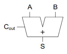
Fig. 1 Half-adder schematic symbol#
The logic equations are:
The cooresponding truth table is shown in Table 1.
\(A\) |
\(B\) |
\(C_{out}\) |
\(S\) |
|
|---|---|---|---|---|
0 |
0 |
0 |
0 |
|
0 |
1 |
0 |
1 |
|
1 |
0 |
0 |
1 |
|
1 |
1 |
1 |
0 |
The Chips#
You will use two TTL chips to build the half adder. Their data sheets are available in Teams.
Connecting the Chips#
We will create a half adder circuit using the following process: Connect the first AND gate from the 74LS08 to the inputs (A) and (B) to produce the Carry output.
Connect the first XOR gate from the 74LS86 to the inputs (A) and (B) to produce the Sum output.
We will get the following combinational logic circuit:
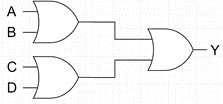
Fig. 2 Half adder implementation#
This setup will give you a half adder circuit, where: Sum (S) is high when exactly one of the inputs is high. Carry (C) is high only when both inputs are high.
Breadboards#
A breadboard is a prototyping device that allows you to easily connect different portions of a circuit together Fig. 3 depicts how the breadboard used in this ICE is connected. Each row (on either side of the center line) is a single node. This means two devices can be connected together by inserting them in the same row. Additionally, each of the columns on the outside of are connected the entire length of the board. These columns are ideal for supplying power and ground to your circuits.
Fig. 3 Breadboard connections#
Build the circuit#
Power Supply#
You will use a USB power supply to power your circuit.
Attach the power supply to the top of the breadboard so the red vertical lines align with the positive pins (+5V and +3.3V) and the blue lines align with the negative pin (ground, 0V) according to Fig. 4.
Note
The breadboard has numbered rows. Make sure your power supply is connected to rows #1-3 or the red and blue rails will be backwards!
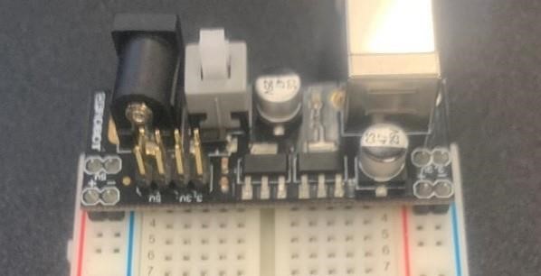
Fig. 4 Power supply placement#
Double check to make sure your power supply is in the right place. Insert the USB cable into your computer. Press the white button to turn on the power supply.
You will use a digital multi-meter (DMM) to test the power supply. Turn the multimeter to the DC voltage setting and place the black lead into the ground rail and the red lead into the 5V rail according to Fig. 5.
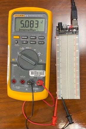
Fig. 5 Testing power supply with DMM#
The meter should read about 5V. Once you have successfully tested, turn off your power supply by depressing the white button.
Switches and Resistors#
Next you are going to configure your input switches. This portion of the circuit will allow us to provide a logic 0 to the circuit (0 V or low) when the switch is not active and a logic 1 to the circuit(5 V or high) when the switch is active.
The switches and resistors are going to be in a pull down configuration or active high.
This means when the switch is open there is a direct connection between the circuit and ground through a resistor which pulls the value to 0.
However, when the switch is closed, the circuit is now connected to the power supply (5 V). This provides a logic 1. We will use 2x \(1 kΩ\) resistors and 2x switches.
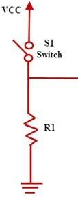
Fig. 6 Pull-down resistor configuration#
Wire the switches according to the graphic below. Ensure your set up accommodates connections to the chips.
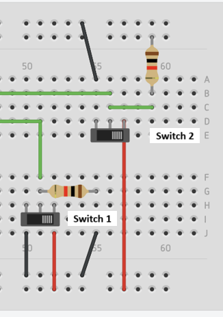
Fig. 7 Switch wiring configuration#
Now you will test the circuit.
Connect the black DMM lead to ground.
Connect the red DMM lead to one of the switches on the “switched” side of the switch (middle node).
Select the DC voltage option on your meter.
Turn on your USB power supply.
Make sure the meter reads about 5V.
Flip (open) the switch.
Make sure the meter reads 0V. This should be pulled hard to 0V, not floating slightly above it!
Repeat this testing for the other switched value (B). When complete, turn off the power supply.
Chip Installation#
Danger
Make sure your power supply is powered off while making changes to the circuit!
You will now add the 74LS08 chip, and the 74LS86 chip. After following these steps, your board should look like Fig. 10.
Power#
Do this for both chips
Place the chip along the center spacing to ensure each lead of the chip is on its own node (and not connected). Note the indentation and orientation of the chip, and be careful to push the chip straight into the board and not bend the pins!
Look at the datasheets to determine which pin on the chip is Vcc.
Wire the Vcc pin to +5V on your bread board.
Repeat for the ground pin.
74LS08#
The chip has four AND gates; we will be using AND gate #1, which uses pins 1, 2, and 3.
Hint
The half circle at the top of the chip helps you know where pin 1 is!
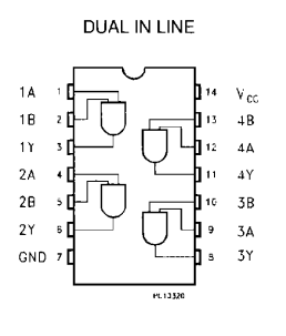
Fig. 8 74LS08 Pin Out (AND)#
Connect the switch 1 (\(A\)) output to pin 1 on the 74LS08.
Connect the switch 2 (\(B\)) output to pin 2 on the 74LS08.
Connect a wire to pin 3 (\(C_{out}\)) on the 74LS08.
See Fig. 10 for a visual.
According to our equation, if both switches are active, the CARRY operation will be high.
Connect the black lead of the DMM to ground and the red lead to the output of pin of the AND gate (Pin 3). Turn on the power and test your circuit by turning both switches on.
Once that works, turn your power back off.
74LS86#
The chip has four XOR gates; we will be using XOR gate #1, which uses pins 1, 2, and 3.
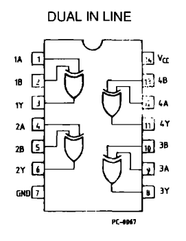
Fig. 9 74LS86 Pin Out (XOR)#
Connect the switch 1 (\(A\)) output to pin 1 on the 74LS86.
Connect the switch 2 (\(B\)) output to pin 2 on the 74LS86.
Connect a wire to pin 3 (\(S\)) on the 74LS08.
See Fig. 10 for a visual.
According to our equation, if any single switch is active, the SUM operation will be high.
Connect the black lead of the DMM to ground and the red lead to the output of pin of the XOR gate (Pin 3). Turn on the power and test your circuit by turning a single switch on.
Once that works, turn your power back off.
Tip
The meter is likely reading closer to 4.5 V and not 5 V.
Fortunately, in both the 74LS08 and 74LS86, anything above 2 V is considered high, or logic 1.
Similarly, anything less than 0.8 V would register as a logic 0.
At this point, your board should look like this:
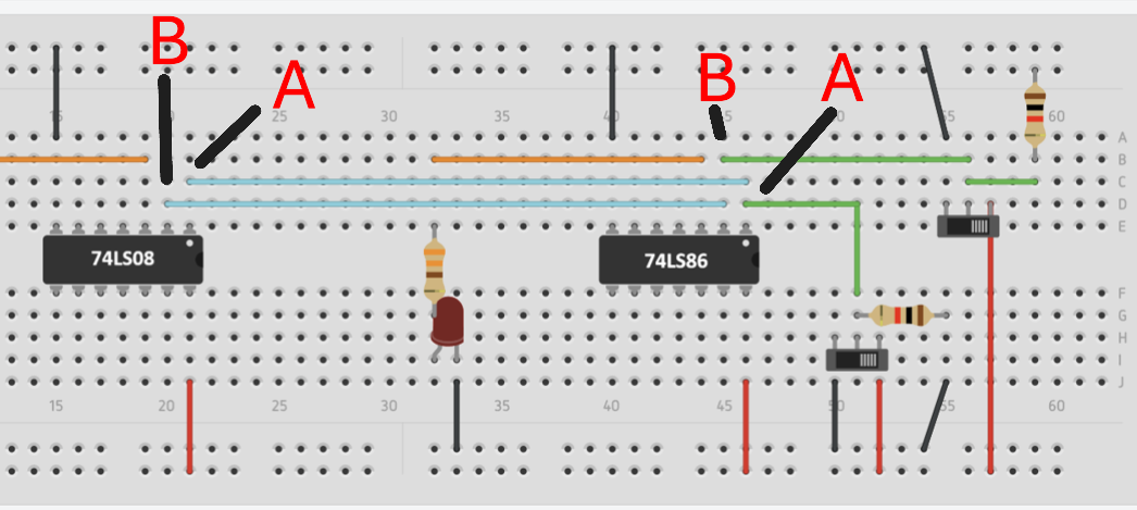
Fig. 10 Chip wiring before adding LEDs.#
Wire LED#
The final step is to wire the LED. This LED will indicate if the
circuit output is a logic 1 (LED is on) or logic 0 (LED is off).
Warning
To keep from destroying the LED due to a potential current spike, you will wire the LED in series with a \(1 kΩ\) resistor.
LEDs are directional components. The longer of the LED’s two leads are where current enters, where the shorter end is where current exits. Place the LEDs across two empty nodes, connecting the shorter ends to ground. Ensure the positive ends are on empty nodes.
Next, connect pin 3 (output pin) of the 74LS08 and 74LS86 to two different empty nodes. Use a 1 kΩ resistor to connect these nodes to the the nodes where the positive ends of the LEDs are connected. You should have a 1 kΩ resistor between the LED and the output pin nodes.
Wire up the LED according to Fig. 11
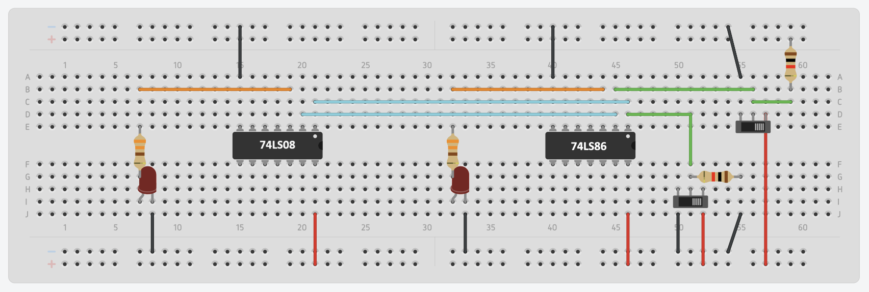
Fig. 11 LED wiring#
For your final test, simply turn on the power and test your switches to ensure they match your half adder logic equations!
Exit Criteria#
Demonstrate your operational circuit to your instructor.
When all switches are off, the LEDs are off.
When any one switch (A or B) is turned on, the LED connected to the 74LS86 will light up.
When both switches (A and B) are turned on, the LED connected to the 74LS08 will light up.