Lab 2 - Seven Segment Display Decoder#
Overview#
In this lab you will implement the seven-segment display decoder in VHDL to display a hexadecimal digit. The hex digit will come from a hardware-based binary to hex converter, which you will develop.
A four-bit value will be input using switches. Upon pressing the center button, a seven-segment display will output the correct hex digit, Fig. 32
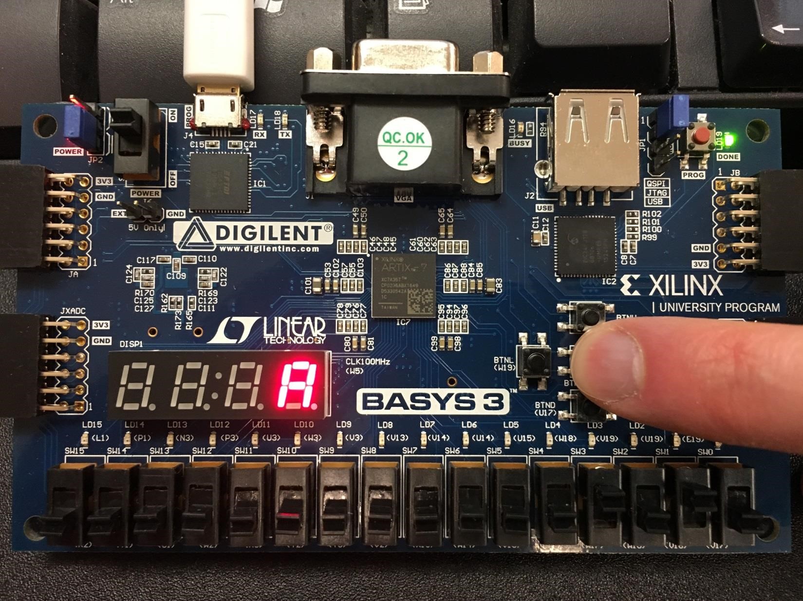
Fig. 32 Binary-to-hex displayed on seven-segment display#
Objectives#
Develop a hardware-based binary to hex converter
Display switch value on seven-segment display
Demo#
Here is a quick demo showing how your seven-segment display decoder should function.
Supplies#
Digilent Basys3 Artix-7 FPGA Development Board
Design Software: Xilinx Vivado 2024.2
Collaboration#
All components of this lab are individual effort, although you can always discuss general concepts with other students.
Note
Do not show other students your working code. If helping another student, you can look at their code to help them troubleshoot it, but refer them to example code in the textbook, lecture slides, etc. to help them resolve the coding issue.
Background#
When creating simple embedded digital designs, a seven-segment display
is a common way to display numbers or simple letters to the end-user. In
this lab, you will design a seven-segment display decoder. This decoder
takes a 4-bit binary input, and produces 7 bits that indicate whether
each “segment” of the display is on (0) or off (1).
There are seven “segments” (labeled a – g, see Fig. 33) and one decimal point (we will ignore the d.p. in this lab) in a seven-segment display.
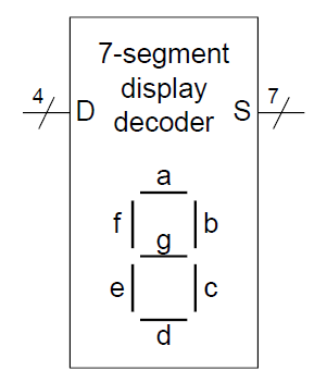
Fig. 33 Labeled segments in display#
On our Basys3 board an anode determines which of the displays are on, while cathodes allow you to turn on each individual segment, Fig. 34
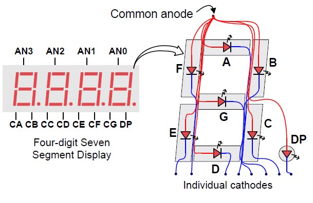
Fig. 34 Basys3 7SD cathodes and anodes.#
Placing a 0 on a segment will cause it to light up, while a 1 will keep the segment dark.
This is called “active low.”
For example, to display the number “0”, a logic 0 must be placed on segments a-f,
while segment g will be a logic 1.
In this way, you can display every hexadecimal digit: “0” - “F” as shown in Fig. 35
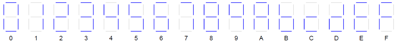
Fig. 35 Hexadecimal digits on a seven-segment display#
Pre-lab#
Thoroughly read Digital Design and Computer Architecture Example 2.10, page 77-81.
Read Basys3 Reference Basic I/O and Seven Segment Display.
Complete the Gradescope Assignment (add rows to truth table and answer hardware questions).
Lab#
It is time to implement the seven segment display decoder in hardware with VHDL!
Setup Vivado Project#
We will be creating our own Vivado project, instead of giving you a pre-made one. See Lab2 Vivado Buttonology.pptx in Class Materials for screenshots!
Go to USAFA-ECE/ece281-lab2
Click the green “Use this template” button -> create a new repository.
Once your new repo is created, clone it into where you want it.
Open Vivado
Follow instructions in Create a new Vivado Project. Name your project binaryHexDisp
Ensure your source hierarchy looks like you expect.
Edit the file headers as necessary. Then commit your changes with git.
Seven Segment Display Decoder#
For better modularity, we will implement our seven segment display decoder as its own component.
Note
You will need to reuse your seven segment display decoder in future labs!
File Creation#
We have not given you a file, so you need to create one in Vivado. See Lab2 Vivado Buttonology.pptx in Class Materials for screenshots!
In the Sources tab click the blue + symbol.
Add or create design sources
+ and Create file
Create file
File type: VHDL
File Name: sevenseg_decoder
File location: your project src/ folder (NOT default “local to project”)
You should then see the file, click Finish.
Define a module:
Entity name:
sevenseg_decoderi_Hex, in, Bus, MSB: 3, LSB: 0o_seg_n, out, Bus, MSB: 6, LSB: 0
You should then see sevenseg_decoder added to Design Sources
Commit this newly created file to git!
Architecture#
Our truth table had \(S_a\) to \(S_g\). How does this map to hardware? Fundamentally, we want to adhere to the constraints file. This is because we will ultimately want to do this:
-- Excerpt from expected sevenseg_decoder port map inside top_basys3
o_seg_n => seg,
Note
We are using o_seg_n because the _n reminds us it’s active LOW!
Returning to Basys3 I/O and comparing it to Basys3_Master.xdc we can see that:
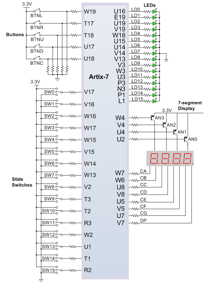
The pin
W7is connected to cathodeCA, which we have calledsA.Basys3_Master.xdcshowsPACKAGE_PIN W7 [get_ports {seg[0]}], sosAis the LSB
Meanwhile,
The pin
U7is connected to cathodeCG, which we have calledsG.Basys3_Master.xdcshowsPACKAGE_PIN U7 [get_ports {seg[6]}], sosGis the MSB
Unfortunately, this is the opposite of our prelab truth table 😭
It’s up to you to decide how to fix this inside sevenseg_decoder!
Tip
The answer to this needs to go in your lab report.
Behavioral vs. Structural modeling#
There are two basic philosophies for modeling digital architectures:
structural describes how the module would be composed as a hierarchy of simpler modules.
behavioral describes what the logic does in terms of inputs and outputs.
We used structural for the adders earlier in this course. We could use it here as well, giving each segment a Boolean equation:
But you’d then have to do this for each of your segments!
For this component, you are probably better off with a behavioral approach. As a reminder, here is the behavioral code for a one-hot decoder.
-- Behavioral model for one-hot decoder
with i_sel select
o_D <=  "0001" when "00",
        "0010" when "01",
        "0100" when "10",
        "1000" when "11",
        "0000" when others;
How might you adapt this for your seven-segment decoder?
Once you do this, commit your file with git.
Test sevenseg_decoder#
Hint
Test bench entities do not have any input or output ports! So when you create the file leave that part blank.
Follow steps similar to above to create a new file, except select Add or create simulation sources.
Name your test bench file sevenseg_decoder_tb.vhd with the entity sevenseg_decoder_tb.
Refer to previous assignments for how to make a test bench. Remember to bring in your sevenseg_decoder component!
Create a test plan to verify your decoder behaves as expected. Don’t forget that you can use hex to assign values to signals.
Once you are happy with your test, add a screenshot of your waveform to your folder and commit it and your other files with git.
top_basys3#
The functionality we are looking for is this:
        flowchart LR
    binary([4-bit input]) --> hex[Convert to hex]
    hex --> button{Display active?}
    button --> out[Display hex output]
The user will:
Input a 4-bit number on switches 3-0.
Expect that value to be output only on display 0 when button C is pressed; otherwise all displays are off.
Design#
Before writing code draw the entity diagram for top_basys3.
Ensure it has all the inputs and outputs you need.
swshould just be four bits (and then only uncomment 0-3 in the constraints file).Include your sevenseg_decoder entity and all connections to internal signals and gates.
DO NOT draw the inner architecture of sevenseg_decoder.
Tip
Your entity I/O names should exactly match the port names already in the Basys3_Master.xdc constraints file.
Implementation#
Now connect everything in VHDL like you show in your diagram.
Using btnC#
The output an is four bits but btnC is only one bit.
The easiest way to connect these is with a signal.
We will append _n to the signal name to remind ourselves it is active LOW.
w_7SD_EN_n  <= not btnC;

an(0)   <= w_7SD_EN_n;
an(1)   <= '1';
an(2)   <= '1';
an(3)   <= '1';
Alternatively, you could do this with some VHDL magic and the () aggregate operator:
an <= (0 => w_7SD_EN_n, others => '1');
Implement in hardware#
Uncomment the relative lines in your constraints file.
Remember to only uncomment sw(0) - sw(3), not all 16 switches.
Synthesize and implement your design. Then generate a bitstream and squirt it to your board.
Commit the bitstream to your repo
Deliverables#
Prelab#
See instructions at the top of this lab. Submit on Gradescope.
Hardware demo#
You have to hold the center push button down for a 7SD to show your output.
The correct hex digit is shown based on the switch positions for all input possibilities.
Demo can be performed live with an instructor (preferred) OR submitted via Teams video.
Written Report#
You are not required write an entire lab report. Only complete the following sections:
Title Section
Introduction
Methodology (VHDL Implementation section only)
In the introduction section, be sure to include how the seven segment display operates at a high level. There should be some discussion of the role of the common anode and the individuals cathodes.
In the VHDL Implementation section, be sure to discuss how your VHDL code addresses the difference in msb/lsb orientation in your prelab truth table compared to the physical connection to the cathodes on the Basys3 board.
Include images and figures as needed to help explain the concepts/code to your reader. If you include a figure, you need to discuss that figure.
Code on Gradescope via GitHub#
sevenseg_decoder.vhdandsevenseg_decoder_tb.vhdincluded insrc/Extraneous comments are removed and code is formatted in a sane manner
Screenshot of testbench waveform
Basys3_Master.xdcappropriately uncommentedBitstream (
.bit) file used for hardware demo in repo (in default location)Commit messages are useful in tracing the development of the project