ICE 3: Ripple-Carry Adder#
HW 12#
Read Overview and Background sections below.
Copy and clone your copy of USAFA-ECE/ece281-ice3
Open
RippleCarryAdder.digand complete it!Ensure the test passes by clicking the Play button with the green check mark (Hovering over it says “Run all test cases in this circuit”).
Git commit, push, submit to Gradescope
Important
When you go to GitHub you must click Use this template and then git clone
your copy of the repository.
If you don’t know if you did that right, open GitBash and use the following command from within that directory. You should see your GitHub username, not USAFA-ECE
# Should show
# origin  https://github.com/YOUR-USERNAME/ece281-ice3.git (fetch)
# origin  https://github.com/YOUR-USERNAME/ece281-ice3.git (fetch)
git remote -v
Clone your copy of the repository
Open the project in Vivado
Modify the headers
Overview#
In this ICE we will make a 4-bit ripple-carry adder.
So far in this course you have implemented individual components on your FPGA. However, one of the benefits of VHDL is that we can pull multiple components into a single design.
In order to organize and reuse individual components, we are introducing the concept of a Top Level Design.
Important
The Top Level is where you pull in and connect all of the different components before finally connecting them to the IO of the board.
This is how you will manage the complexity of combining numerous components.
You will need to use the concept of a Top Level Design in Lab 2, so this is directly applicable.
Objectives#
The objectives of this in-class exercise are for you to:
Implement and test a ripple-carry adder with full adders using VDHL
Employ a
top_level.vhdfileGain more experience using tools (Git, Markdown, Xilinx Vivado)
Demo#
Here is a quick demo showing how your 4-bit ripple carry adder should function.
Background#
Full Adder#
A full adder extends the half-adder to include a Carry In bit, \(C_{in}\).
Tip
Adders are discussed on page 238 of Digital Design and Computer Architecture, RISC-V Ed.
A truth table, schematic symbol, and logic equations for a full-adder are shown below.
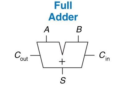
Fig. 17 Full-adder schematic, from fig 5.3 in DDCA#
\(C_{in}\) |
\(A\) |
\(B\) |
\(C_{out}\) |
\(S\) |
|
|---|---|---|---|---|---|
0 |
0 |
0 |
0 |
0 |
|
0 |
0 |
1 |
0 |
1 |
|
0 |
1 |
0 |
0 |
1 |
|
0 |
1 |
1 |
1 |
0 |
|
1 |
0 |
0 |
0 |
1 |
|
1 |
0 |
1 |
1 |
0 |
|
1 |
1 |
0 |
1 |
0 |
|
1 |
1 |
1 |
1 |
1 |
Ripple-Carry Adder#
The simplest way to build an \(N\)-bit carry propagate adder is to chain together \(N\) full adders.
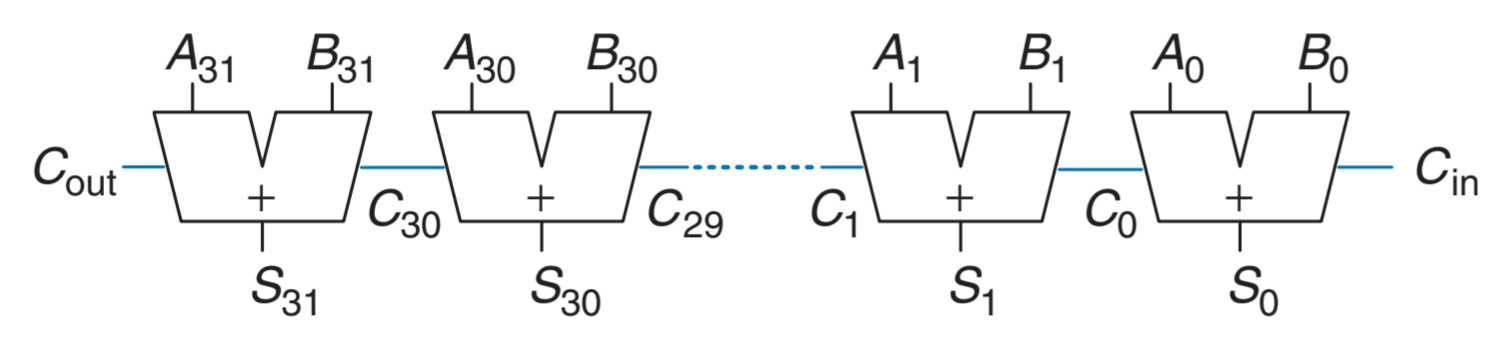
Fig. 18 *DDCA Figure 5.5 shows a 32-bit ripple carry adder.#
Our goal will be to implement this in VHDL!
The Project#
Setup Vivado#
You’ve already cloned the repository, so you should be able to simply open the .xpr!
Notice that we have include a Full Adder for you. It’s very similar to the Half Adder you made for ICE 2!
Ripple-Carry Adder VHDL#
First, open RippleCarryAdder.dig from your Homework.
Then, in Vivado, open ripple_adder.vhd and verify that the entity matches what you’d expect based on your Digital simulation.
Declarations#
Full Adder Component#
Declare a full_adder component declaration to ripple_adder.vhd between the architecture and begin statements.
The full adder component must match the entity declaration in full_adder.vhd.
Hint
These port names match the names from HW 12’s Digital!
architecture Behavioral of ripple_adder is

    component full_adder is
        port (
            A     : in std_logic;
            B     : in std_logic;
            Cin   : in std_logic;
            S     : out std_logic;
            Cout  : out std_logic
            );
        end component full_adder;
This is like saying “go find the entity that matches this description and get it ready to use!”
Signal Declaration#
Remember, signals are like wires between inputs and components.
We will need the following signals:
A carry signal to carry the ripple between adders.
Replace the ? with the appropriate number (look at your Digital schematic!!) and copy this signal declaration into ripple_adder.vhd
signal w_carry : STD_LOGIC_VECTOR(? downto 0); -- for ripple between adders
Instantiations#
Now that we have made the full_adder component available to use within ripple_adder we need to instantiate multiple occurrences of the component and declare the logic to connect them to each other and to inputs/outputs.
Remember, we are trying to build what’s in your schematic, which is the 4-bit version of Fig. 18. Thus, we are going to use four Full Adders… just like in your Digital schematic!
Here are the first two instantiations of full_adder. Notice that each has a unique name (because of the number at the end) and is connected slightly differently.
Copy this code into ripple_adder.vhd below the begin statement.
-- PORT MAPS --------------------
    full_adder_0: full_adder
    port map(
        A     => A(0),
        B     => B(0),
        Cin   => Cin,   -- Directly to input here
        S     => S(0),
        Cout  => w_carry(0)
    );

    full_adder_1: full_adder
    port map(
        A     => A(1),
        B     => B(1),
        Cin   => w_carry(0),
        S     => S(1),
        Cout  => w_carry(1)
    );
Then add the other two full adder instantiations.
Ripple-Carry Test#
Open ripple_adder_tb.vhd.
The component has already been declared and instantiated for you.
Do some quick math… how many possible inputs are there to our 4-bit adder? More than we want to manually input! 😄
Fill out the remainder of the test bench with a few cases. Strive for decent coverage by:
The min and max cases (input all zeros and all ones)
The easy-to-forget cases (such \(0 + 0 + C_{in} = 1\))
A few random ones from the middle.
Get a passing simulation before moving on!
At this time commit and push your files to GitHub
Tip
Incremental testing may seem slower, but it will save you time in the long run!
top_basys3#
Important
From now on, we will use a top level design file as the boundary of our system.
It allows us to connect internal components and our I/O in a reliable manner.
We will name the top-level file top_basys3.vhd… because it’s the top file for our Basys 3 board!
Open that file now.
Previously, you edited Basys3_Master.xdc to match your entity.
Going forward, we will leave the xdc defaults and only uncomment the ports we need.
You’ll find that this will reduce errors and increase reusability.
For example, our Basys3_Master.xdc has the following default for switches,
which we can use as a std_logic_vector:
set_property PACKAGE_PIN V17 [get_ports {sw[0]}]
    set_property IOSTANDARD LVCMOS33 [get_ports {sw[0]}]
Entity#
Tip
You actually, really, really need to sketch this before coding it!
Also, this is what the Instructor TB in Gradescope checks.
Our user will input the following on switches (sw):
\(C_{in}\) on switch 0
\(A\) on switches 4-1
\(B\) on switches 15-12
Our user will expect the following outputs on LEDs (led):
\(Sum\) on LED 3-0
\(C_{out}\) on LED 15
Sketch this entity and how sw and led connect to ripple_adder.
Then, and only then, ensure you see the following in your top_basys3.vhd:
entity top_basys3 is
    port(
        -- Switches
        sw  :   in  std_logic_vector(15 downto 0);

        -- LEDs
        led :   out std_logic_vector(15 downto 0)
    );
end top_basys3;
Architecture#
Declare a ripple_adder component.
Instantiate the ripple_adder component.
Connect the switches and LEDs appropriately.
Test#
You could make a top_basys3_tb.vhd and test it, but we’ve already tested
the full_adder and we wouldn’t gain much more information.
Let’s just move onto deploying to the board!
Note
If we had multiple components in our top_basys3, we should definitely make a testbench. This is called integration testing, as opposed to the unit testing that we are currently doing.
Implement Design#
Constraints File#
Open Basys3_Master.xdc.
Because we used the appropriate naming conventions in top_basys3.vhd you should not change the names!
Simply uncomment all the sw and led lines.
Test bitstream on FPGA#
Synthesize, implement, generate.
Squirt the bitstream to the board, and be amazed!
Deliverables#
See GitHub real fast if you need some tips.
README#
Take a screenshot of your ripple_adder waveform, save it to the root of your directory.
Make the screenshot appear in your README with the following Markdown syntax:

Now do the same with your sketch of the top_basys3 entity that you made earlier (it can be a quick and dirty picture).
Add a ## Documentation section to the README. This is the only
one you need for the entire ICE; you don’t need one in the file headers.
## Documentation

My statement here.
Add the image and README.md to git and commit.
Other files#
Run
git statusDouble check that you have the image, your README.md and all
.vhdand.bitfiles committed to your git repo.Then push them to your repo.
Make sure all your work appears in GitHub as you expect.
Submit the assignment on Gradescope.
Make sure the autograder in Gradescope passes!
Congratulations, you have completed In Class Exercise 3!