Lab 1 - ThirtyOneDayMonth#
Due: Lesson 11
Overview#
In this lab you will design a circuit that takes a month as a 4-bit
binary input (e.g., January is equivalent to 0001 and December is
equivalent to 1100). For each month that has 31 days, you should turn on
the red LED (your output value, \(Y\), is 1). All other months should produce an output of 0
and unused inputs can produce an output of X (don’t care).
You will design several prototypes, simulate some of those prototypes, and then implement one design in hardware.
This circuit will first be implemented in hardware using integrated circuits and then implemented in hardware using VHDL.
Objectives#
Design and implement a circuit in hardware using integrated circuits.
Design and implement a circuit in hardware using VHDL.
Supplies#
5x \(1 kΩ\) resistors
1x red LED
1x 74x151 8:1 MUX IC
1x 74x04 INVERTER (NOT) IC
1x breadboard power supply
1x breadboard
4x single pole double throw switches
Jumper wires
Digilent Basys3 Artix-7 FPGA Development Board
Design Software: Xilinx Vivado 2024.2
Collaboration#
Each student must submit his or her own work to Gradescope.
You should collaborate during the pre-lab to figure out how to do the schematics.
The lab itself will be less collaborative, although you can always discuss general concepts with other students.
You can never look at another student’s code.
Per the dean, a Documentation Statement is always required.
Background#
In order to represent 12 months in unsigned binary, we know we need four bits:
Eventually we will move to representing that with a vector, but for now let’s just give each input bit a letter: \(A\), \(B\), \(C\), \(D\), from most to least significant bit.
Our output is \(Y\).
If input month has 31 days then \(Y=1\)
If input month does not have 31 days then \(Y=0\)
If input is not a month then \(Y=X\) (don’t care)
Pre-lab#
The pre-lab will be submitted to Gradescope prior to starting the lab.
Go to USAFA-ECE/ece281-lab1
Click “Use this template” and make a repository under your GitHub account
Use Git Bash to clone the newly-created repository to your local machine
Verify that you’re using your copy of the repository not the USAFA-ECE one
# Run this from inside your lab 1 repo
# You will have to `cd` after `git clone`
git remote -v
Important
All prelab work for this assignment must be committed to the prelab/ folder.
Your instructor will not be able to see any other folders in Gradescope.
Boolean Equations#
Note
These instructions leave off file extensions.
You can use whatever you want, as long as Gradescope supports it,
but .pdf or .png is probably the best choice.
Truth Table#
Create a truth table that represents the conditions described above. Use https://www.tablesgenerator.com/markdown_tables
It should have the following columns
Month
Input \(A\)
Input \(B\)
Input \(C\)
Input \(D\)
Output \(Y\)
Here are the first two rows
Month |
A |
B |
C |
D |
Y |
|---|---|---|---|---|---|
0 |
0 |
0 |
0 |
X |
|
Jan |
0 |
0 |
0 |
1 |
1 |
Hint
You can think of A, B, C, D as a 4-bit vector.
In this case, A is the most significant bit (MSB) while D is the least-significant bit (LSB).
Insert this truth table under the Truth Table heading in prelab/README.md
K-Map#
Use a K-map to find the simplified equation for \(Y\).
Add your k-map to the repository at
prelab/kmap(with an appropriate file extension). Then commit your k-map.Write your simplified boolean equation under the Boolean Equation heading in
prelab/README.md
Draw schematics#
So far with the engineering method we’ve defined the problem. The next steps are to “collect data,” “create viable solutions,” and “analyze solutions and select the best solution.”
Available chips#
Collecting data == determining what chips we have available.
Our lab has the following 7400 series transistor-transistor logic (TTL) integrated circuits (IC)
74151 8:1 MUX
7404 Inverter (NOT)
74159 4:16 One-Hot Decoder
7432 2-input OR
7400 4-input NAND
7411 3-input AND
These data sheets are available in Teams or can be searched online.
Create viable solutions#
We will iterate to hone in on the best solution.
First we will draw designs with logic gates
Next we will draw some of those designs with IC schematics
Then we will simulate some of those designs
Finally, we will build one design.
Hand Drawn Logic Gates#
Do this before doing the simulations below.
Using logic gate symbols that correspond to the types of chips you have available draw four separate schematics that can implement your truth table. Make sure to reference data sheets for the components to ensure you have included every input they need to function
Tip
It is much easier to draw circuits with logic gates than with IC schematics. We are looking to prototype so we can quickly compare alternatives.
Even though we are being fast here, strive to be as neat as possible. See Digital Design and Computer Architecture Figure 2.23 for a great example.
DO NOT draw the inner architecture of the chips! For example, the MUX should just be a trapezoid.
The circuits should be four files saved as either .png or .pdf.
The first schematic will use an 8:1 MUX and NOT gates. –> name this file
MUXThe second schematic will use a 4:16 “one-hot” decoder and OR gates. –> name this file
DecoderThe third schematic will use NOT gates, AND gates, and OR gates. –> name this file
SOPThe fourth schematic will use only NAND gates. –> name this file
NAND
Place your hand-drawn schematics into
prelab/and add/commit them with git.
Simulated Logic Gates#
Now that you have four prototypes to compare, we will rule out some solutions and continue with two viable options.
Typically, this is an involved process (often with a decision matrix!) But for our purposes, we will pick for you.
Use Digital to simulate the following two circuits.
We give you templates in prelab/.
8:1 MUX and NOT –>
MUX.digNOT, AND, OR –>
SOP.dig
Important
DO NOT delete any of the components in the provided templates. Even if you don’t use the component, leave it in the file. The autograder is checking for these components and running a simulation assuming all these components (to include inputs) are within the .dig file. You will fail the autograder test if you delete them.
After you have working simulations, commit your changes!
IC Schematics#
With two working simulations, it’s time to decide which circuit we are actually going to build.
In Digital, simulate the a 8:1 MUX (74151) and inverter (if using) (7404)
as an IC schematic using the prelab/MUX_74151.dig template.
Hint
Look at the datasheet!
Some of the chips must be powered (Vcc or Gnd)
as well as enabled (see “strobe”).
Pay attention to the order of the inputs to the MUX and encoder; which bit is the MSB?
You will build this IC on a breadboard directly off of this simulation!
Prelab Deliverables#
Your prelab submission will only include files in the prelab/ folder;
all other files will be ignored by Gradescope!
Commit your changes to your repository.
Push all your changes to GitHub.
Verify that your changes show up in your repository.
Submit to Gradescope Prelab 1 assignment
Verify that Gradescope autograder is happy
Lab: Integrated Circuit#
Using your Digital simulation of the first schematic (8:1 MUX (74151) and inverter(s) (7404)) you will implement Thirty-One Day Month functionality in hardware using integrated circuits.
Tip
Remember to avoid floating inputs, or you will spend a lot of time debugging.
All unused input pins need to be grounded (0) or connected to Vcc (1).
Danger
Do not connect unused outputs to Ground; this will cause a short and let out the magic smoke!
Power down your circuit before making any adjustments or changes!
Reference ICE 1: Breadboard Half Adder if you need a refresher on how the breadboard functions and how to place your power converter. You can also reference the breadboard handout in the Datasheets Library to determine how the breadboard is connected.
Double check all connections before turning on power.
Demo your operational integrated circuit to an instructor.
Commit an image of your circuit to your git repo.
Lab: FPGA#
Now we will construct the same circuit in VHDL.
Setup Vivado Project#
Open the .xpr file with Vivado.
You should see the following files:
thirtyOneDayMonth.vhdthirtyOneDayMonth_tb.vhdBasys3Master_Lab1.xdc
Tip
You can optionally enable GitHub Actions in your repository. Doing so will enable your simulation to run on every push to the repo.
While you are also running simulations in Vivado, this will be useful because it gives you confidence that the Gradescope autograder will be happy.
Additionally, this continual testing is a big piece of DevOps.
Entity#
Create your interface (ports) for the thirtyOneDayMonth according to Fig. 31.
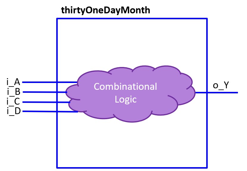
Fig. 31 thirtyOneDayMonth entity with interfaces shown in blue and architecture in purple.#
Think of this as the actual chip we used in the integrated circuit. The internal architecture is purple. It is a cloud because we haven’t defined the circuitry inside that makes the chip do the desired combinational logic.
The ports can be created in VHDL using the std_logic signal type.
Remember, std_logic is like a single digital logic wire.
Input interface#
You found the logic equation during the pre-lab.
Let’s map the input \(A\) from that equation to i_A in our entity.
Recall that the i_ prefix matches the naming convention for inputs described in the header.
i_A : in std_logic;
Use the above syntax to create the rest of the input ports within the entity.
Output interface#
Our pre-lab output \(Y\) was a single bit; likewise, the output, o_Y
is a single wire, so will still be of the std_logic type.
o_Y : std_logic;
Use the above syntax to create the output port within the entity.
You now have the entity portion of the thirtyOneDayMonth component complete. Next, you need to develop the internal logic, the architecture.
Architecture#
Now that we have our entity interfaces, it’s time to describe the internal behavior of our circuit.
Create the logic to implement the internals of the thirtyOneDayMonth entity. The logic is described using VHDL, but the Basys3 board will implement the design using logic gates and other hardware components similar to what is inside the chip used during the integrated circuit portion of the lab.
As we saw in class, a multiplexer has 3 different signals: select, input, and output. We will connect three of our entity inputs to select bits and the fourth input bit to the input of the multiplexer. The entity output will be used as the multiplexer output.
Since we already created the entity inputs and outputs, the only internal
signal we need to implement is the select.
This can be created using the std_logic_vector signal type as seen below.
This is declared before begin:
signal w_sel : std_logic_vector (2 downto 0); -- MUX sel
Hint
A std_logic_vector signal is a vector of std_logic signals; meaning, you can access a wire within the vector using an index inside of parentheses.
Replace the example code to include the multiplexer select signal within the architecture.
In the CONCURRENT STATEMENTS section of the architecture you will need
to connect your entity inputs to the appropriate wires of the w_sel
vector. The individual wires of a vector can be accessed with indexes.
To assign a value to the LSB of the vector you would do the following:
w_sel (0) <= i_C ; -- connect input C to the LSB of w_sel
Repeat the signal assignment for
i_Bto index 1 andi_Ato index 2.
Finally, implement your prelab design using behavioral modeling as discussed in class.
Testbench and Simulation#
The testbench will be used to simulate your entity prior to implementing it on the Basys3 board. As you will learn, implementation takes a very long time and simulating your solution will save you a lot of headache.
The general concept of a testbench is to include the component you created and then test every input and observe if the output matches the truth table designed in the prelab.
As this is the first time using a testbench, a lot is spelled out for you. Read through the provided template to see how it was set up. In the future you will have to write a lot of this code. There are three main sections that are complete to pay attention to:
Component: declares the component of your top-level entity (this is the unit under test, UUT). This section will be an exact copy of your entity.
Additional components: These are internal signals used to wire your simulated inputs and outputs to the entity. You will typically need a wire that corresponds to each port of your top-level entity.
Port Maps: A port map wires your internal signals to the entity. There should be a port map for each entity you are testing.
A 4-bit test signal vector, w_sw, was created for you in the Additional
components section to create your test cases. Instead of assigning each
bit of the entity (A-D), you can assign all 4 inputs at once using hex.
For example, you can use x"1" to represent the binary "0001" which
would then assign a 1 to i_D and a 0 to i_A through i_C. Since we are
simulating real hardware, we will have to create delays between each
change in input. We can test an input and delay for 10 ns using the
following:
w_sw <= x"0"; wait for 10 ns;
This is the first test case of our 4-bit input truth table. To finish the test process, you need to create the additional \(2^4 - 1\) lines.
Complete the test process
Run the simulation#
After the testbench is written, under SIMULATION click Run Simulation.
When the waveform appears, maximize the window. Then, edit the names of the i_sw bits as \(A\), \(B\), \(C\), and \(D\), to help match the results to your truth table.
Click the > to expand the vector. Then right click on [3] and select rename.
You can then change it to i_A. Repeat for the other three signals.
Make sure the simulation results match your truth table.
Constraints File#
Open your Basys3Master_Lab1.xdc file.
The .xdc file maps the signals in your entity to the physical pins on the board. This time the constraints file is complete and you will not need to make changes to it.
As an example, i_A is mapped to pin W17 which is the 4th switch from the right.
The other inputs are mapped similarly.
The output, o_Y is mapped to pin U16 which corresponds to the
LED on the far right.
In the future, you will have to ensure the mapping is done correctly.
Implement#
Generate the bitstream (.bit) file and download it to your FPGA.
Verify that your design functions correctly.
Deliverables#
Prelab#
See instructions at the top of this lab. Submit on Gradescope.
Hardware Demo#
Demo your working integrated circuit to your instructor.
Demo your working Basys3 board to your instructor.
Demo can be performed live with an instructor (preferred) OR submitted via Teams video.
Written Report#
You are not required to write an entire lab report. Only include the following sections:
Title Section
Abstract
Follow the template and rubric on Teams. Upload the required lab report sections to Gradescope as a single .pdf file.
Code on Gradescope via GitHub#
Commit all images,
.vhd,.bit, and.xdcfiles to your repoPush your changes to GitHub
Submit to Gradescope and verify you get full points from the autograder