Lesson 14 – Transistors and Digital Logic#
Learning Outcomes#
Explain what a transistor is and describe its function.
Identify the basic structure and operation of a transistor.
Construct logic gates using transistors.
Calculate the number of transistors required for a logic gate.
Develop truth tables from logic diagrams.
Introduction#
In Block 1, you analyzed circuits with voltages and currents that could take on a continuous range of values — a resistor might drop 3.7 V, a current might be 42 mA. That world is called analog. In this lesson, we make a deliberate simplification that turns out to be enormously powerful: we restrict our voltages to just two possible states.
Logic 0 (LOW) — the voltage is near zero
Logic 1 (HIGH) — the voltage is near the supply voltage
That’s it. By agreeing to only care about two states, we gain something huge: noise immunity and perfect reproducibility. A signal that drifts to 4.8 V instead of 5.0 V is still unambiguously a 1. This binary world is the foundation of every computer, phone, and digital system you’ve ever used.
The device that makes this possible is the transistor — a semiconductor switch that can be turned ON or OFF by an electrical signal. Everything in digital electronics, from a simple logic gate to a 19-billion-transistor CPU, is built from this one idea.
Transistor Fundamentals#
A transistor is a three-terminal semiconductor device that controls current flow. In ECE 315 we focus on its role as a switch: a small electrical signal at one terminal controls whether current flows between the other two. In this way, transistors act as electronically controlled valves.
Transistors are fabricated from doped semiconductor material. By introducing controlled impurities into silicon, we create two types of regions:
N-type — excess electrons are the majority carriers
P-type — “holes” (absence of electrons) are the majority carriers
How these regions are arranged determines the transistor type. The two most important families are the Bipolar Junction Transistor (BJT) and the Field-Effect Transistor (FET).
Bipolar Junction Transistor (BJT)#
A Bipolar Junction Transistor (BJT) uses both electrons and holes to conduct current — hence the name bipolar. It is formed by sandwiching three doped regions together, creating either an NPN or PNP structure.
Structure#
The three terminals of a BJT are:
Emitter — heavily doped; injects charge carriers into the device
Base — thin and lightly doped; acts as the control region
Collector — collects the carriers that flow through the base
In an NPN transistor, the emitter and collector are N-type and the base is P-type. In a PNP transistor, the arrangement is reversed.

Fig. 1. NPN BJT structure showing N-type emitter and collector with a P-type base.
Fig. 2. PNP BJT structure showing P-type emitter and collector with an N-type base.
Operation#
The BJT is a current-controlled device. A small current injected into the base, \(I_B\), allows a much larger current to flow between the collector and emitter, \(I_C\). This amplifying relationship is captured by:
where \(\beta\) is the current gain of the transistor. For digital applications, we only care about two operating points:
\(I_B = 0\) → transistor is OFF (open switch)
\(I_B > 0\) → transistor is ON (closed switch)
The BJT is excellent for discrete amplifier circuits, but it always draws some base current, which adds up when you have millions of devices. This is why modern digital chips use FETs instead.
Field-Effect Transistor (FET)#
A Field-Effect Transistor (FET) controls current using an electric field rather than a current. This makes it a voltage-controlled device — and since the control input draws negligible current, FETs are far more power-efficient than BJTs at scale.
FETs are unipolar: conduction relies on only one type of carrier (either electrons or holes).
Structure#
The three terminals of a FET are:
Source — where charge carriers enter the channel
Drain — where charge carriers exit the channel
Gate — applying a voltage here creates an electric field that opens or closes the channel
The most important FET variant for digital systems is the MOSFET (Metal-Oxide-Semiconductor FET). Two complementary types are used:
NMOS — N-channel MOSFET; turns ON when gate voltage is high
PMOS — P-channel MOSFET; turns ON when gate voltage is low
Modern chips use CMOS (Complementary MOS) technology, which pairs NMOS and PMOS devices together. This arrangement draws significant current only during switching transitions, dramatically reducing static power consumption compared to earlier technologies.
Operation#
The gate voltage \(V_{GS}\) (measured between gate and source) determines whether the channel conducts:
\(V_{GS} < V_{th}\) → transistor is OFF
\(V_{GS} \geq V_{th}\) → transistor is ON
where \(V_{th}\) is the threshold voltage — the minimum gate voltage needed to open the channel. Because the gate is separated from the channel by a thin oxide layer, it draws essentially no steady-state current. This is what makes MOSFETs suitable for microprocessors, memory, and any high-density integrated circuit.
Comparison: BJT vs. FET#
Characteristic |
BJT |
FET |
|---|---|---|
Control Mechanism |
Current-controlled (\(I_B\)) |
Voltage-controlled (\(V_{GS}\)) |
Carrier Type |
Bipolar (electrons and holes) |
Unipolar (one carrier type) |
Input Current |
Requires base current |
Negligible gate current |
Power Efficiency |
Higher power consumption |
Lower power consumption |
Primary Modern Use |
Amplifiers, discrete circuits |
Integrated circuits, CPUs |
The bottom line: BJTs are still widely used in analog circuits and discrete applications, but virtually every digital system you encounter today — from a microcontroller to a GPU — is built on CMOS FET technology.
Semiconductor Carrier Model for Switching#
To understand why a small base signal enables a large collector current, it helps to think about what is happening at the carrier level. In an NPN device, the base region sits between the emitter and collector. Without base drive, the P-type base creates a barrier that blocks electron flow. When a small current is injected into the base, it modifies that barrier just enough to allow a much larger stream of electrons to flow from emitter to collector.
Fig. 3. Conceptual carrier model illustrating how base drive enables conduction between collector and emitter.
This is the physical mechanism behind the switch. In digital design, we don’t need to track individual carriers — we just need to know that base current controls the ON/OFF state, which is all the abstraction below requires.
Transistor as an Ideal Switch#
Rather than analyzing carrier physics every time, digital logic uses a clean abstraction: the transistor behaves like an electrically controlled switch.
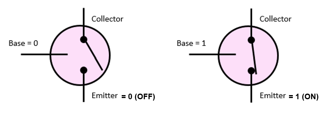
Fig. 4. Idealized switch model of a transistor controlled by the base input.
When the control input is LOW (0), the switch is open and no current flows — the output is LOW. When the control input is HIGH (1), the switch closes and current flows — the output is HIGH. This gives us a simple input-output relationship:
Base Input |
Output |
|---|---|
0 |
0 |
1 |
1 |
With this abstraction in hand, we can analyze networks of transistors using nothing more than series/parallel circuit reasoning — the same tools you already know from Block 1.
Truth Tables#
Before building logic gates, we need a systematic way to describe what a digital circuit does for every possible input. That tool is the truth table: a complete listing of all possible binary input combinations and the corresponding output for each.
For a circuit with \(n\) independent binary inputs, there are exactly \(2^n\) possible input combinations. Two inputs give 4 rows; three inputs give 8 rows; four inputs give 16 rows. Each added input doubles the table size.
Truth tables are the standard language for specifying, analyzing, and verifying digital logic functions.
Logic Gates from Transistor Switch Networks#
By wiring transistor switches in series and parallel, we implement the fundamental logical operations. There are only three primitive gates needed to build any logic function: AND, OR, and NOT.
AND Gate — Series Configuration#
If you wire two switches in series, current can only reach the output when both switches are closed. That is exactly the AND function.
Fig. 5. Two-switch series network implementing an AND function.
\(A\) |
\(B\) |
Out |
|---|---|---|
0 |
0 |
0 |
0 |
1 |
0 |
1 |
0 |
0 |
1 |
1 |
1 |
The output is 1 only when both A and B are 1. In Boolean notation:
The schematic symbol has a flat left edge (inputs) and a rounded right edge (output). No bubble means no inversion. Whenever you see a flat-left, curved-right symbol without a circle, it’s an AND gate.
Fig. 6. AND-gate schematic symbol.
OR Gate — Parallel Configuration#
Two switches in parallel provide a conduction path whenever either switch is closed — that’s the OR function.
Fig. 7. Two-switch parallel network implementing an OR function.
\(A\) |
\(B\) |
Out |
|---|---|---|
0 |
0 |
0 |
0 |
1 |
1 |
1 |
0 |
1 |
1 |
1 |
1 |
The output is 1 whenever at least one input is 1. The only way to get a 0 out is if both inputs are 0. In Boolean notation:
The OR gate symbol has a concave (curved inward) left edge and a pointed right edge. The curved input side signals that any input can drive the output high.
Fig. 8. OR-gate schematic symbol.
NOT Gate — Inverter#
The NOT gate has a single input and produces its logical complement. Where an AND or OR gate combines multiple inputs, the NOT gate simply flips the one it receives.
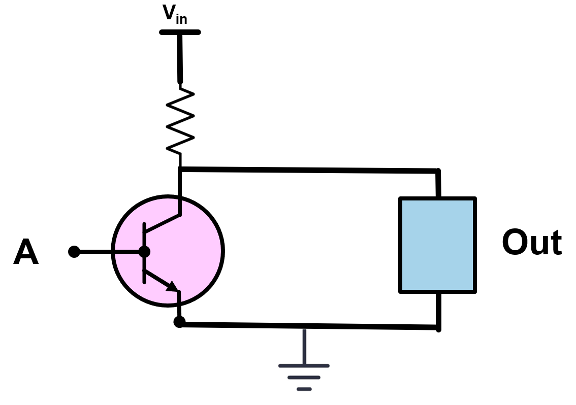
Fig. 9. Inverter (NOT) concept circuit using a transistor switch abstraction.
\(A\) |
Out |
|---|---|
0 |
1 |
1 |
0 |
With only one input, there are \(2^1 = 2\) rows. The output is always the opposite of the input. In Boolean notation:
The symbol is a triangle (representing signal flow) with a small circle — called an inversion bubble — at the output. That bubble is the universal indicator of logical inversion. When you see it on the output of an AND or OR gate, it produces a NAND or NOR function, respectively.

Fig. 10. NOT-gate (inverter) schematic symbol.
Transistor Count and Scaling#
Every logic gate requires a certain number of transistors. Complex computation emerges from combining large numbers of simple gates, so transistor count is a useful measure of circuit complexity.
Device |
Transistors |
|---|---|
NOT gate |
1 |
2-input AND gate |
2 |
2-input OR gate |
2 |
6502 CPU (early Apple computer) |
4,528 |
Apollo 11 CPU |
17,000 |
1st Gen F-16 CPU |
110,000 |
PlayStation 2 |
53,500,000 |
First iPhone CPU |
125,000,000 |
iPhone 16 CPU |
19,000,000,000 |
Intel i9-13900K CPU |
26,000,000,000 |
Each row in that table represents the same fundamental idea repeated at a different scale. A modern CPU contains 26 billion transistors doing nothing more exotic than switching ON and OFF very quickly and in very large numbers.
The circuit below implements a half-adder — a circuit that adds two single-bit inputs \(A\) and \(B\) and produces a Sum output and a Carry output. How many transistors does it require?

Fig. 11. Half-adder logic diagram — the circuit whose transistor count is being determined.
Understand: Each logic gate type has a known transistor cost. We just need to count the gates and multiply.
Identify Key Information:
NOT gate = 1 transistor each
2-input AND gate = 2 transistors each
2-input OR gate = 2 transistors each
Plan: Count each gate type in the diagram, multiply by its transistor cost, and sum the results.
Solve:
Gate Type |
Count |
Transistors Each |
Subtotal |
|---|---|---|---|
NOT |
2 |
1 |
2 |
AND (2-input) |
3 |
2 |
6 |
OR (2-input) |
1 |
2 |
2 |
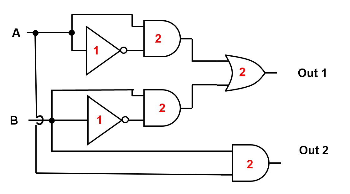
Fig. 12. Half-adder circuit with gate counts and transistor subtotals annotated.
Answer: This half-adder circuit requires 10 transistors.
Multi-Input Logic Gates#
AND and OR gates are not limited to two inputs. A 3-input AND gate, for example, outputs 1 only when all three inputs are 1 — the same rule, just extended. The transistor count scales with the number of inputs: an \(n\)-input AND or OR gate requires \(n\) transistors.
For a logic gate (or circuit) with \(n\) independent binary inputs, the number of rows in the truth table is:
Each additional input doubles the number of combinations: 2 inputs → 4 rows, 3 inputs → 8 rows, 4 inputs → 16 rows.
3-Input AND Gate#
Fig. 13. 3-input AND gate schematic symbol.
For inputs \(A\), \(B\), and \(C\), there are \(2^3 = 8\) combinations. The AND rule is unchanged: the output is 1 only when every input is 1.
\(A\) |
\(B\) |
\(C\) |
Out |
|---|---|---|---|
0 |
0 |
0 |
0 |
0 |
0 |
1 |
0 |
0 |
1 |
0 |
0 |
0 |
1 |
1 |
0 |
1 |
0 |
0 |
0 |
1 |
0 |
1 |
0 |
1 |
1 |
0 |
0 |
1 |
1 |
1 |
1 |
3-Input OR Gate#
Fig. 14. 3-input OR gate schematic symbol.
The OR rule extends equally: the output is 1 whenever at least one input is 1. The only row that produces a 0 is the one where all inputs are 0.
\(A\) |
\(B\) |
\(C\) |
Out |
|---|---|---|---|
0 |
0 |
0 |
0 |
0 |
0 |
1 |
1 |
0 |
1 |
0 |
1 |
0 |
1 |
1 |
1 |
1 |
0 |
0 |
1 |
1 |
0 |
1 |
1 |
1 |
1 |
0 |
1 |
1 |
1 |
1 |
1 |
Analyzing Logic Diagrams#
When a logic diagram combines multiple gates, the approach is always the same: trace signals stage by stage from inputs to output, evaluating one gate at a time. Write intermediate results as you go and fill in the truth table row by row.
Given the logic diagram below, determine the output Out for all input combinations of \(A\) and \(B\).
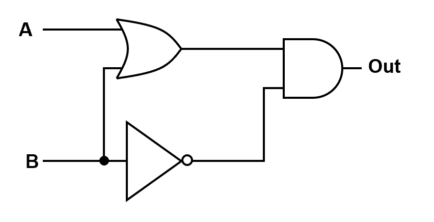
Fig. 15. Logic diagram for Example Problem 2: OR and NOT gates feed into a final AND gate.
Understand: There are two inputs, so we have \(2^2 = 4\) rows to evaluate. Trace each input combination through the circuit one gate at a time.
Identify Key Information:
The OR gate takes \(A\) and \(B\) as inputs
The NOT gate takes only \(B\) as its input
The AND gate combines the OR output and the NOT output to produce Out
Plan: For each row: compute the OR output, compute the NOT output, then AND them together.
Solve:
Row 1: \(A = 0\), \(B = 0\)
OR: \(0 \text{ OR } 0 = 0\)
NOT: \(\text{NOT}(0) = 1\)
AND: \(0 \text{ AND } 1 = \mathbf{0}\)
Row 2: \(A = 0\), \(B = 1\)
OR: \(0 \text{ OR } 1 = 1\)
NOT: \(\text{NOT}(1) = 0\)
AND: \(1 \text{ AND } 0 = \mathbf{0}\)
Row 3: \(A = 1\), \(B = 0\)
OR: \(1 \text{ OR } 0 = 1\)
NOT: \(\text{NOT}(0) = 1\)
AND: \(1 \text{ AND } 1 = \mathbf{1}\)
Row 4: \(A = 1\), \(B = 1\)
OR: \(1 \text{ OR } 1 = 1\)
NOT: \(\text{NOT}(1) = 0\)
AND: \(1 \text{ AND } 0 = \mathbf{0}\)
\(A\) |
\(B\) |
Out |
|---|---|---|
0 |
0 |
0 |
0 |
1 |
0 |
1 |
0 |
1 |
1 |
1 |
0 |
Answer: Out = 1 only when \(A = 1\) and \(B = 0\).
Notice what’s happening: the NOT gate forces the AND gate’s second input to 1 only when \(B = 0\). The AND gate then requires the OR output to also be 1, which needs at least one of \(A\) or \(B\) to be 1. The only way both conditions are met simultaneously is \(A = 1\), \(B = 0\). The circuit effectively implements: A is true while B is false.
Fig. 16. Example Problem 2 circuit with intermediate signal values labeled at each stage.
Given the logic diagram below, determine the output Out for all input combinations of \(A\) and \(B\).
Fig. 17. Logic diagram for Example Problem 3: AND gate output feeds one input of the OR gate alongside B.
Understand: Inputs \(A\) and \(B\) feed an AND gate. That AND output, along with \(B\) directly, feed an OR gate to produce Out.
Identify Key Information:
AND stage: combines \(A\) and \(B\)
OR stage: combines the AND output with \(B\)
Note that \(B\) feeds into both stages
Plan: For each of the 4 input combinations, evaluate the AND gate first, then the OR gate.

Fig. 18. Example Problem 3 circuit with the AND stage output labeled as an intermediate signal.
Solve:
Row 1: \(A = 0\), \(B = 0\)
AND: \(0 \cdot 0 = 0\)
OR: \(0 + 0 = \mathbf{0}\)
Row 2: \(A = 0\), \(B = 1\)
AND: \(0 \cdot 1 = 0\)
OR: \(0 + 1 = \mathbf{1}\)
Row 3: \(A = 1\), \(B = 0\)
AND: \(1 \cdot 0 = 0\)
OR: \(0 + 0 = \mathbf{0}\)
Row 4: \(A = 1\), \(B = 1\)
AND: \(1 \cdot 1 = 1\)
OR: \(1 + 1 = \mathbf{1}\)
\(A\) |
\(B\) |
Out |
|---|---|---|
0 |
0 |
0 |
0 |
1 |
1 |
1 |
0 |
0 |
1 |
1 |
1 |
Answer: Out = 1 whenever \(B = 1\), regardless of \(A\).
This is a great example of why tracing signal paths matters. Because \(B\) feeds directly into the OR gate, whenever \(B = 1\) the output is forced to 1 — the AND stage becomes irrelevant. When \(B = 0\), the AND gate cannot produce a 1 (anything AND 0 = 0), so the OR gate sees two 0s and outputs 0. Despite having two gates in the circuit, the whole thing simplifies to \(\text{Out} = B\).
Given the logic diagram below, determine the output Out for all input combinations of \(A\), \(B\), and \(C\).

Fig. 19. Logic diagram for Example Problem 4: OR gate feeding into a 3-input AND gate alongside B and C.
Understand: Three inputs means \(2^3 = 8\) rows. The circuit has two stages: an OR gate first, followed by a 3-input AND gate.
Identify Key Information:
OR stage: takes \(A\) and \(B\)
AND stage: takes the OR output, plus \(B\) and \(C\) directly
Plan: For each row, compute the OR output from \(A\) and \(B\), then evaluate the 3-input AND gate using (OR result), \(B\), and \(C\).
Solve:
\(A\) |
\(B\) |
\(C\) |
OR(\(A\),\(B\)) |
AND(OR, \(B\), \(C\)) = Out |
|---|---|---|---|---|
0 |
0 |
0 |
0 |
0 |
0 |
0 |
1 |
0 |
0 |
0 |
1 |
0 |
1 |
0 |
0 |
1 |
1 |
1 |
1 |
1 |
0 |
0 |
1 |
0 |
1 |
0 |
1 |
1 |
0 |
1 |
1 |
0 |
1 |
0 |
1 |
1 |
1 |
1 |
1 |
\(A\) |
\(B\) |
\(C\) |
Out |
|---|---|---|---|
0 |
0 |
0 |
0 |
0 |
0 |
1 |
0 |
0 |
1 |
0 |
0 |
0 |
1 |
1 |
1 |
1 |
0 |
0 |
0 |
1 |
0 |
1 |
0 |
1 |
1 |
0 |
0 |
1 |
1 |
1 |
1 |
Answer: Out = 1 only when \(B = 1\) and \(C = 1\).
Notice that changing \(A\) has no effect on the output — the two rows where \(B = 1\) and \(C = 1\) produce Out = 1 regardless of whether \(A\) is 0 or 1. This tells you that \(A\) is not part of the effective logic condition. Even though three inputs enter the circuit and the OR gate is present, the circuit simplifies to \(\text{Out} = B \cdot C\). Recognizing when an input has no influence on the output is an important pattern-recognition skill in digital logic design.
Summary#
Transistors are the fundamental building blocks of all digital systems. A small electrical signal at the control terminal switches the device between a fully ON state and a fully OFF state — and that simple behavior, repeated billions of times, is what makes computation possible.
In this lesson you built up the complete picture from device physics to working logic circuits:
BJTs are current-controlled devices (\(I_C = \beta I_B\)); FETs are voltage-controlled (\(V_{GS}\) vs. \(V_{th}\)). Both act as switches in digital applications, but MOSFETs dominate in integrated circuits because they draw negligible gate current.
Transistors are abstracted as ideal switches — ON when the control input is 1, OFF when it is 0. This lets us analyze digital circuits using series/parallel reasoning.
AND behavior comes from switches in series — all must be closed.
OR behavior comes from switches in parallel — any one closed is sufficient.
NOT inverts the input; its symbol carries an inversion bubble to mark the complement.
A circuit with \(n\) inputs has \(2^n\) truth table rows, and each added input doubles the count.
Complex logic diagrams are analyzed by tracing signals stage by stage. Watch for inputs that feed directly into OR gates — they can dominate the output and simplify the apparent function considerably.
Transistor count is a practical measure of circuit complexity, and the exponential scaling of modern fabrication technology is what puts 19 billion transistors on a chip the size of a fingernail.
Key Takeaways#
Transistor as a switch. A transistor is a three-terminal semiconductor device that acts as an electrically controlled switch, forming the fundamental building block of all digital logic.
BJT (Bipolar Junction Transistor). A current-controlled device where a small base current \(I_B\) enables a much larger collector current \(I_C = \beta I_B\); used primarily in analog and discrete circuits.
FET/MOSFET. A voltage-controlled device that turns on or off based on the gate-to-source voltage \(V_{GS}\) relative to a threshold voltage \(V_{th}\); draws negligible gate current, making it the dominant technology in integrated circuits.
CMOS technology. Pairing complementary NMOS and PMOS transistors reduces static power consumption and is the basis of virtually every modern digital chip.
Logic gates from switch networks. AND gates arise from transistors in series (all must conduct), OR gates from transistors in parallel (any one conducting is sufficient), and NOT gates invert a single input.
Truth tables. A complete listing of all \(2^n\) input combinations and their corresponding outputs for a circuit with \(n\) binary inputs; the standard tool for specifying and verifying digital logic behavior.
Inversion bubble. The small circle on a gate symbol’s output universally indicates logical inversion; its presence on AND or OR gates produces NAND or NOR functions, respectively.
Transistor count scaling. Complex logic functions are built by combining large numbers of simple gates, and modern fabrication places tens of billions of transistors on a single chip by repeating the same ON/OFF switching principle at enormous scale.
