
Lesson 25 – Analog-to-Digital Conversion 2#
Learning Outcomes
Design signal conditioning between a transducer and an ADC to avoid aliasing, clipping, and a mismatch of dynamic ranges.
Calculate the bit rate of an ADC system and determine either how much memory is needed to store data for a specified duration, or how long an ADC will take to fill a memory card of a specified size.
Analog-to-Digital Conversion: Bit Rates and Signal Conditioning#
When we design systems that include ADCs, we often characterize them by how much data they provide per second — this is known as the ADC bit rate.
Bit Rates#
The bit rate is straightforward to calculate: multiply the number of bits produced per sample (\(b\)) by the total number of samples per second (\(f_s\)):
Key Concept
Using the bit rate, we can determine how much memory is needed to store a certain amount of data, or how much data we can store on a given memory card. Data rates are often given in bits per second (bps) or kilobits per second (kbps), while storage is measured in bytes (B):
With bytes, instead of one kilobyte equaling \(10^3\) bytes, it is defined as \(2^{10}\) bytes. The most common conversions are:
Signal Conditioning#
Typically, ADCs come with a fixed sampling frequency, dynamic range, and resolution. To ensure we avoid aliasing and clipping, we must condition the input signal before it reaches the ADC.
Consider the 8-bit ADC below, used in a voice recorder to digitize a microphone signal. The microphone outputs range from \(-10\ \text{mV}\) to \(10\ \text{mV}\).
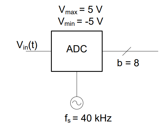
Fig. 1. 8-bit ADC with 40 kHz sampling rate.
We must first ensure aliasing is avoided. The Nyquist criterion requires:
With \(f_s = 40\ \text{kHz}\):
To guarantee this, it is common practice to add a low-pass (anti-aliasing) filter before the ADC, with cutoff frequency:

Fig. 2. Anti-aliasing filter used with an 8-bit ADC.
Now, consider whether the ADC will accurately resolve the signal. The resolution is:
The microphone’s entire range (\(-10\ \text{mV}\) to \(10\ \text{mV}\)) falls within a single ADC level — the ADC cannot distinguish any variation in the microphone output. The solution is a transducer interface that amplifies the signal to span the full ADC range. Since both ranges are symmetric around zero:
When the signal is not centered on the ADC range, the interface must also shift it with a DC bias, \(B\). As in Lesson 20, the interface output is:
Match the two ends of the input range to the two ends of the ADC range to find both values:
For the microphone, both ranges are centered on zero, so \(B = 0\).
Fig. 3. Transducer and anti-aliasing filter used with an 8-bit ADC.
Properly designing the transducer interface avoids two pitfalls:
Clipping — when the input exceeds \(V_{\max}\) or falls below \(V_{\min}\), the ADC saturates at all 1s or all 0s, losing information.
Wasted resolution — when the signal spans only a fraction of the ADC range, most levels go unused.
Finally, all data produced by the ADC must be stored. With \(f_s = 40\ \text{kHz}\) and \(b = 8\) bits:
Over one hour:
Converting to megabytes:
A 256 MB memory card is sufficient for one hour of recording.
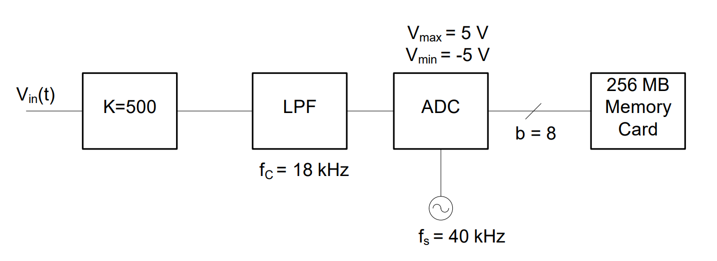
Fig. 4. Complete signal conditioning and memory unit used with an ADC.
Example Problem 1
An accelerometer measures G loading on an aircraft. Its signal passes through a gain-of-1000 amplifier, an anti-aliasing filter, and a 4-bit ADC (\(f_s = 10\ \text{kHz}\), \(V_{\min} = -2\ \text{V}\), \(V_{\max} = 8\ \text{V}\), \(f_c = 5\ \text{kHz}\)), then into a 512 MB flight data recorder (FDR). At three instants, the accelerometer outputs \(490\ \mu\text{V}\), \(7.8\ \text{mV}\), and \(-2.4\ \text{mV}\). What voltage enters the ADC at each instant, are there any problems, and how long until the FDR is full?
Understand: This is a complete signal-chain problem. We need to check for aliasing and clipping, then calculate the recording time limit.
Identify Key Information:
Knowns: \(K = 1000\), \(f_s = 10\ \text{kHz}\), \(b = 4\ \text{bits}\), \(V_{\min} = -2\ \text{V}\), \(V_{\max} = 8\ \text{V}\), \(f_c = 5\ \text{kHz}\), FDR = 512 MB
Unknowns: Voltages at ADC input, validity of design, recording time
Assumptions: None.
Plan: Check aliasing via the Nyquist criterion, check clipping by comparing amplified voltages to the ADC range, then compute bit rate and recording time.
Solve:
Aliasing check: \(f_c = 5\ \text{kHz} = f_s / 2\) — the LPF is correctly designed; aliasing is prevented.
Clipping check: Amplified voltages:
Sample 3 causes clipping — the ADC outputs \(0000_2\) regardless of the actual input. To fix this, the gain, \(V_{\min}\), or the bias \(B\) must be adjusted.
Recording time:
Answer: Samples 1 and 2 are valid. Sample 3 clips because the amplified voltage (\(-2.4\ \text{V}\)) falls below \(V_{\min}\). The FDR can store approximately 29.8 hours of data.
ADC Demo#
The ADC Demo from Lesson 24 has a Signal Conditioning panel with the same tools used in this lesson: a gain \(K\), a bias \(B\) (labelled b in the demo), and an anti-aliasing LPF. Start with a signal that uses only a small part of the ADC range, then adjust the gain and bias until it fills the range without clipping. The demo reports how much of the dynamic range you are using as you go.
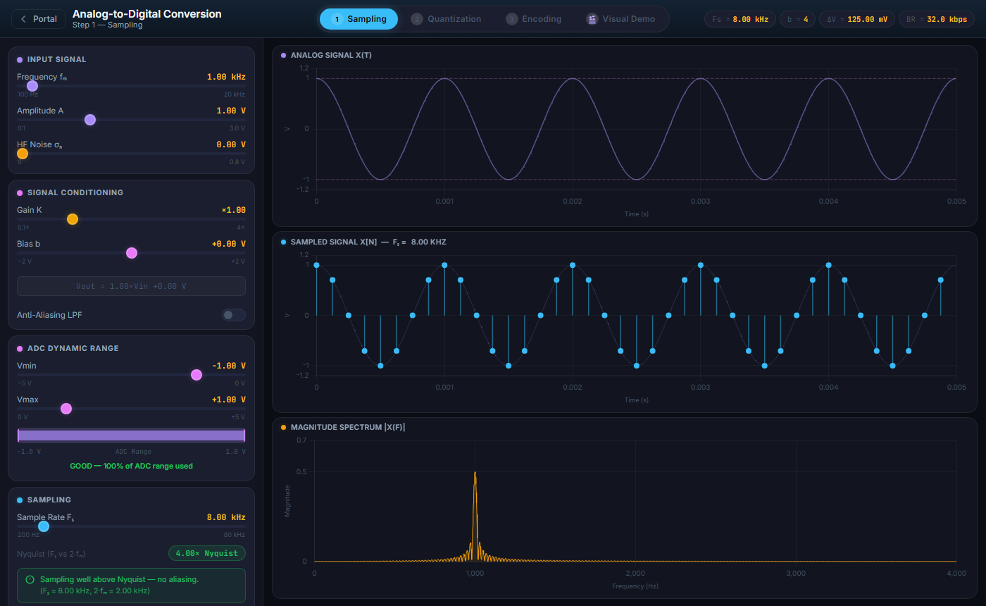
The ADC Demo. The Signal Conditioning and ADC Dynamic Range panels are on the left. Select the image to launch the demo.
Key Takeaways#
ADC bit rate. The bit rate equals the number of bits per sample multiplied by the sampling frequency (\(\text{bit rate} = b \cdot f_s\)) and determines how fast data is produced by the ADC system.
Memory capacity planning. Knowing the bit rate allows you to calculate how much storage is required for a given recording duration, or conversely how long a fixed-size memory card will last.
Anti-aliasing filter. A low-pass filter placed before the ADC with a cutoff frequency at or below \(f_s / 2\) prevents high-frequency content from aliasing into the digitized signal.
Transducer interface (amplifier). When the sensor’s output voltage range is much smaller than the ADC’s dynamic range, a gain stage is required to scale the signal up so that the ADC levels are fully utilized and resolution is not wasted.
Clipping. If the amplified signal exceeds \(V_\text{max}\) or falls below \(V_\text{min}\), the ADC saturates and produces an incorrect output code, losing information irreversibly.
Wasted resolution. A signal that spans only a small fraction of the ADC’s dynamic range uses only a handful of levels, effectively throwing away most of the ADC’s precision — matching the gain to the dynamic range is essential for good performance.
Signal chain design. A complete ADC system must address aliasing (anti-aliasing filter), dynamic range mismatch (amplifier), and data storage (memory sizing) as a coordinated design problem rather than treating each in isolation.