Lesson 17 – Computer Architecture#
Learning Outcomes
By the end of this lesson, you should be able to:
Explain the major components of computer architecture: processor, memory, and I/O devices.
Describe how stack overflow occurs and why it matters.
Differentiate among the three types of system buses: address bus, data bus, and control bus.
Compare and contrast the Central Processing Unit (CPU) and the Graphics Processing Unit (GPU).
The Von Neumann Model — A System View#
Lesson 16 introduced memory and the fetch–decode–execute cycle. In this lesson we zoom out and look at how all the pieces fit together: how the processor, memory, and the outside world communicate, and why the architecture of the processor itself matters enormously for performance.
Modern computer systems are built on the Von Neumann Architecture, which places one key constraint on the entire system: instructions and data share the same memory and the same communication pathways. Everything flows through the same channels.
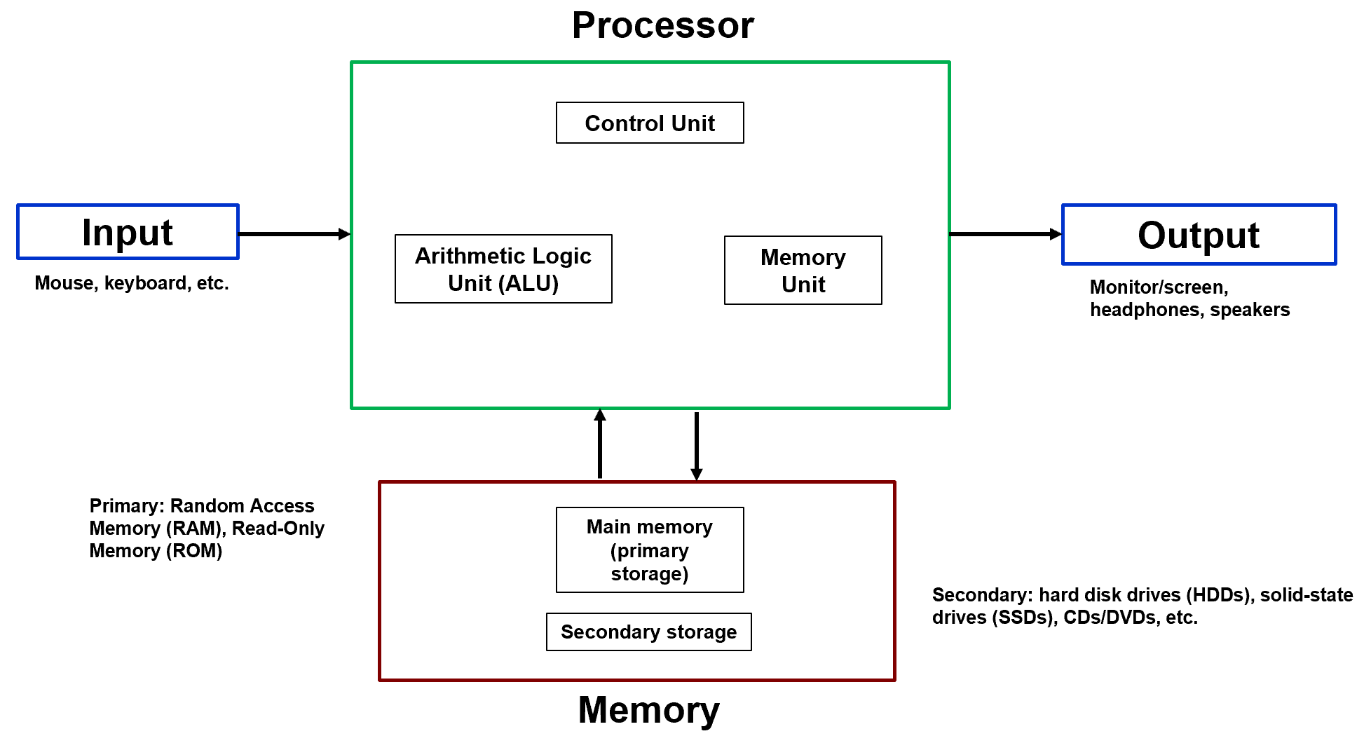
Fig. 1. The Von Neumann Architecture — processor, memory, and I/O devices sharing a common bus.
This shared-pathway design is what creates the Von Neumann Bottleneck — the CPU can only send or receive one thing at a time over the bus. Understanding that constraint is what motivates every major architectural decision in this lesson.
The Central Processing Unit (CPU)#
The CPU is the brain of the system. It continuously performs the fetch–decode–execute cycle, pulling instructions from memory, interpreting them, and acting on them. The CPU does not permanently store programs — it retrieves them from memory one instruction at a time.
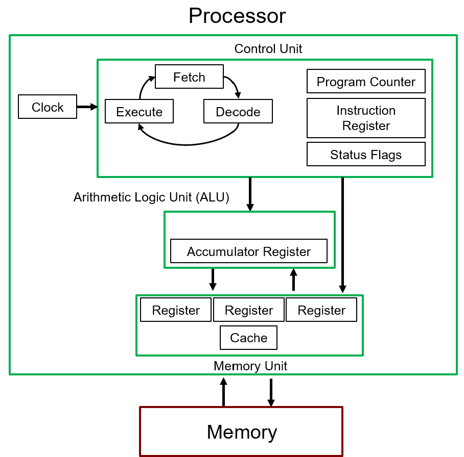
Fig. 2. Internal components of a CPU: Control Unit, Clock, ALU, and Registers/Cache.
Four internal components make this possible:
Control Unit#
The Control Unit (CU) is the conductor of the orchestra. It manages the Program Counter, the Instruction Register, and status flags to determine which instruction executes next, whether execution proceeds sequentially or branches to a new address, and when each internal component needs to act. Without the Control Unit, the processor would have no sense of order.
Clock#
The clock provides the timing signal that synchronizes everything. Measured in Hertz (Hz), each clock pulse coordinates data movement, register updates, and bus transactions. A faster clock means more fetch–decode–execute cycles per second — up to the point where heat and signal integrity become limiting factors.
Arithmetic Logic Unit (ALU)#
The ALU is where all computation happens. It executes arithmetic operations (ADD, SUB, MUL), logical operations (AND, OR, NOT), and comparisons. When engineers talk about a processor’s raw compute power, they are largely talking about the ALU’s throughput.
Registers and Cache#
Registers are the fastest storage in the system — small, directly accessible by the ALU, and used to hold operands, intermediate results, and memory addresses during active computation. Cache is a larger but still very fast memory bank inside the CPU that bridges the speed gap between registers and main (DRAM) memory. Modern CPUs have multiple cache levels (L1, L2, L3), each progressively larger and slower.
Memory Architecture#
Memory stores both program instructions and data values — the stored-program concept from Lesson 16. The system divides memory into two broad tiers.
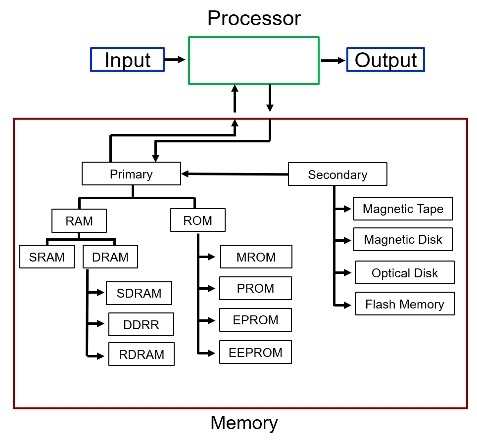
Fig. 3. Memory hierarchy: primary memory (RAM/ROM) is directly accessible by the CPU; secondary storage must be loaded into RAM before execution.
Primary memory (main memory) is directly accessible by the CPU. It holds currently executing programs and their active data. RAM is volatile — it loses its contents when power is removed — and comes in two forms: DRAM for large-capacity main memory, and SRAM for fast cache. ROM is non-volatile and holds permanent firmware.
Secondary memory stores data long-term: SSDs, hard drives, flash storage. The processor cannot execute instructions directly from secondary storage — data must first be loaded into RAM before the CPU can work with it. This is the delay you notice when an application “loads”: the OS is copying the program from secondary storage into primary memory.
The Stack and Stack Overflow#
One important region of primary memory is the stack — a section of RAM reserved for function execution. Every time a function is called, the processor pushes a stack frame onto it containing local variables, function parameters, and the return address (so the CPU knows where to go when the function finishes). When the function returns, that frame is popped off.
A stack overflow occurs when a program attempts to use more stack memory than has been allocated. Common causes are infinite recursion (a function that keeps calling itself without a base case) and deeply nested function calls with large local variables. The consequences range from program crashes and data corruption to exploitable security vulnerabilities — an attacker who can overflow the stack can potentially overwrite the stored return address and redirect execution to arbitrary code.
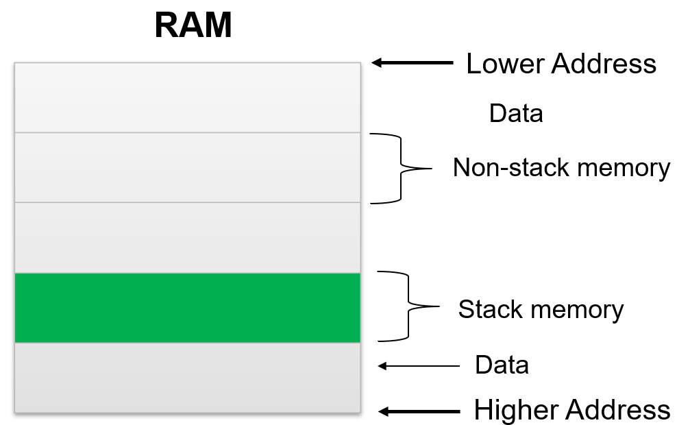
Fig. 4. Stack overflow: repeated function calls push frames onto the stack until allocated memory is exhausted.
The System Bus#
The processor, memory, and I/O devices communicate through a shared set of electrical pathways called the system bus. Three functionally distinct buses work together for every transaction.

Fig. 5. The system bus — address, data, and control buses connecting the CPU, memory, and I/O devices.
Address Bus#
The address bus carries location information — it specifies where in memory (or which I/O device) the current operation targets. It is unidirectional: only the CPU drives the address bus. The width of the address bus determines how many unique locations can be addressed (\(N\) address lines → \(2^N\) locations).
Data Bus#
The data bus carries the actual information being transferred — instructions being fetched, data being read from memory, values being written to an output device. Unlike the address bus, the data bus is bidirectional: data flows from memory to CPU during reads and from CPU to memory during writes.
Control Bus#
The control bus coordinates the transaction. It carries signals that indicate whether the current operation is a read or write, which device has permission to use the bus, and when the transfer is valid. Without the control bus, the address and data buses would be meaningless — the system would have no way to know what to do with the signals on them.
Input and Output#
I/O devices allow the processor to interact with the outside world. Keyboards, monitors, network adapters, and sensors all connect through I/O interfaces (USB ports, HDMI, PCIe slots, etc.) that translate between the device’s native signaling and the bus protocol.
All communication ultimately reduces to binary signals — high voltage (logic 1) and low voltage (logic 0) — with the ordering and timing defined by communication protocols.
Example Problem 1 — Tracing a Keyboard Button Press
Walk through what happens, at the hardware level, when a user presses the letter “J” on a keyboard.
Understand: A key press starts as a physical event and ends as a stored value in RAM and a displayed character on screen. Trace every bus transaction in between.
Solve:
Step 1 — Key Press: You press “J.” The keyboard’s internal circuit detects the physical action and encodes it as a digital signal representing the key’s scan code.
Step 2 — I/O Interface: The keyboard passes the signal through its USB interface, which packages it into a standardized USB protocol frame and forwards it toward the CPU.
Step 3 — Interrupt: The USB controller sends an interrupt signal to the CPU over the control bus. This tells the processor: new input is available. The CPU pauses its current task and turns its attention to the keyboard.
Step 4 — Address: The CPU places the address of the USB keyboard interface on the address bus, signaling: I am ready to read from this device.
Step 5 — Data transfer: The keyboard interface puts the encoded value of “J” onto the data bus. The CPU reads it.
Step 6 — Write to RAM: The CPU writes the received value to a specified memory location over the data bus and address bus. The key press is now stored in RAM.
Step 7 — Display: If the application requires the character to appear on screen, the CPU places the output value on the data bus, addresses the display adapter, and the monitor’s interface reads the data and renders the character.
Answer: A single key press touches all three buses, two I/O interfaces, and RAM — coordinated by the control bus and paced by the clock. The entire sequence takes microseconds.
USB Differential Signaling#
USB does not transmit data on a single wire. It uses differential signaling over two wires, D+ and D−, where the logical state is determined by the voltage difference between them — not the absolute voltage of either wire alone. When D+ is high and D− is low, that represents one logical state; flipping them represents the other. This approach improves noise immunity because external interference tends to affect both wires equally, canceling out in the difference measurement.
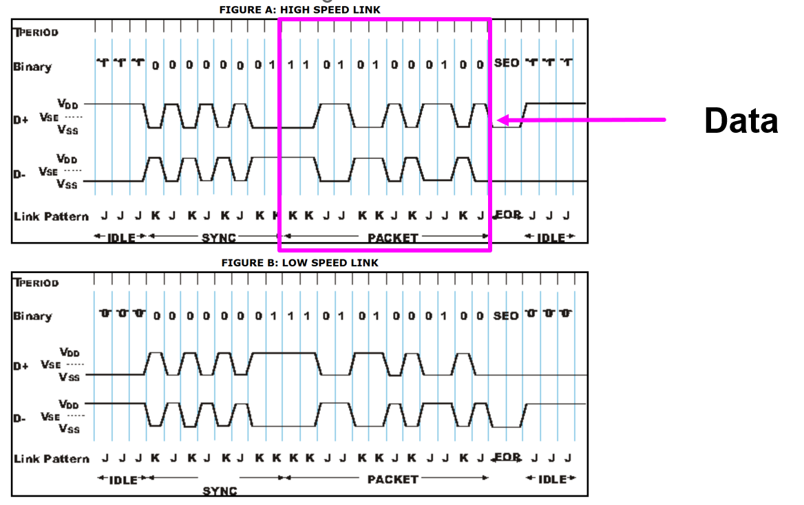
Fig. 6. USB differential signaling: logical state is determined by the voltage difference between D+ and D−, not the absolute voltage of either wire.
The voltage transitions you see in a USB waveform diagram — toggling between \(V_{DD}\) and \(V_{SS}\) — are not just communication artifacts. They are the physical origin of the data that eventually becomes stored charge in DRAM cells. The differential voltage change on the USB lines is interpreted as a binary value, placed on the data bus, addressed to a memory location, and written into the capacitors of a DRAM array. The physical layer of communication connects directly to the memory architecture from Lesson 16.
CPU vs. GPU#
Both CPUs and GPUs perform computation, but they are designed for fundamentally different types of workloads. Understanding why requires looking at how their silicon is allocated.
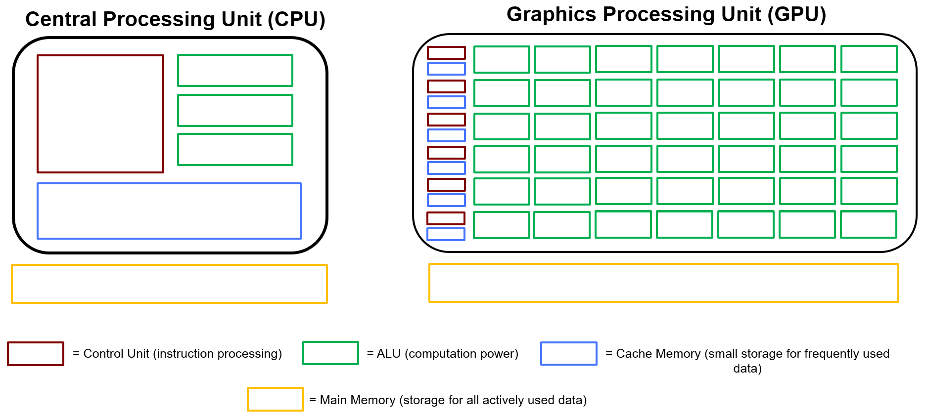
Fig. 7. CPU vs. GPU silicon allocation: CPUs devote most transistors to control logic and cache; GPUs devote most transistors to ALUs for parallel computation.
The diagram above shows how the two processors distribute their transistors across four functional areas: control logic (red), ALUs (green), cache (blue), and main memory interface (yellow).
Feature |
CPU |
GPU |
|---|---|---|
Function |
General-purpose, branch-heavy tasks |
Structured, massively parallel tasks |
Processing model |
Sequential (with limited parallelism) |
Thousands of operations simultaneously |
Core count |
2–64 high-capability cores |
Thousands of simpler cores |
Control logic |
Large — complex branch prediction and scheduling |
Minimal per core |
Cache |
Large — reduces main memory latency |
Smaller, distributed |
Best for |
Operating systems, decision logic, complex programs |
Matrix math, graphics, machine learning |
Why the CPU Is Built the Way It Is#
A CPU devotes a large fraction of its silicon to the Control Unit and cache. This reflects its design goal: handle unpredictable, branch-heavy workloads efficiently. Operating systems, compilers, game logic, and any program with frequent if/else decisions require rapid instruction redirection and sophisticated scheduling. The CPU’s large control logic and branch prediction hardware exist to handle this complexity without stalling. Fewer, more powerful ALUs mean each core can run complicated single-threaded code quickly.
Why the GPU Is Built the Way It Is#
A GPU devotes most of its silicon to ALUs and uses minimal control logic per core. This reflects its design goal: execute the same mathematical operation across enormous datasets simultaneously. Rendering a frame means computing the same shading equation for millions of pixels. Training a neural network means multiplying enormous matrices. These workloads are highly structured and predictable — the GPU doesn’t need sophisticated branching hardware because the same instruction runs on thousands of elements at once. Massive parallelism more than compensates for the simplicity of each individual core.
Consider matrix multiplication:
Each element of \(C\) can be computed independently — there’s no dependency between them. A CPU would compute them sequentially; a GPU computes them all at once across thousands of cores.
The Architectural Tradeoff#
The CPU and GPU are complements, not competitors. Modern systems use both: the CPU manages coordination, branching, and operating system tasks; the GPU handles any structured, numerically intensive workload that can be parallelized. Matching the computation to the right processor is one of the most important performance decisions in system design.
Key Takeaways#
Control Unit. The component of the CPU that manages the Program Counter, Instruction Register, and status flags to sequence instruction execution and handle branching decisions.
System bus. Three functionally distinct buses connect the CPU, memory, and I/O: the unidirectional address bus specifies locations, the bidirectional data bus carries information, and the control bus coordinates read/write operations and device access.
Stack and stack overflow. Every function call pushes a frame of local variables and a return address onto a reserved region of RAM called the stack; exhausting that region (often from infinite recursion) causes a stack overflow, which can crash the program or create a security vulnerability.
Primary vs. secondary memory. Primary memory (RAM/ROM) is directly accessible by the CPU at high speed; secondary storage (SSDs, hard drives) holds data long-term but must be loaded into RAM before the CPU can execute it.
USB differential signaling. USB transmits data using the voltage difference between two wires (D+ and D−) rather than the absolute voltage on either wire, improving noise immunity by canceling out interference that affects both wires equally.
CPU design philosophy. CPUs devote most transistors to control logic and cache to handle unpredictable, branch-heavy workloads efficiently with a small number of powerful general-purpose cores.
GPU design philosophy. GPUs devote most transistors to ALUs with minimal control logic per core, enabling thousands of simple operations to execute simultaneously on structured, parallel workloads such as matrix math and graphics rendering.