Lesson 16 – Computer Memory#
Learning Outcomes
By the end of this lesson, you should be able to:
Explain the physical implementation of computer memory.
Differentiate between Dynamic Random Access Memory (DRAM), Static Random Access Memory (SRAM), and Read-Only Memory (ROM).
Apply fundamental concepts of assembly language and machine code.
Calculate Program Counter (PC), Instruction Register (IR), Accumulator, and RAM address values during the fetch–decode–execute cycle.
The Von Neumann Architecture#
Every computer you have ever used — from a smartphone to a supercomputer — is built on the same fundamental design model: the Von Neumann Architecture. Proposed in the mid-20th century, it organized the computer into four primary components connected by shared communication pathways.
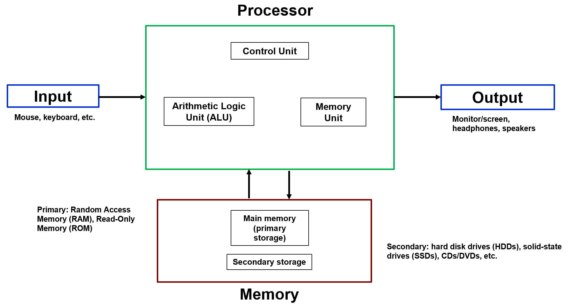
Fig. 1. Von Neumann Architecture block diagram: Input, Processor (CPU), Memory, and Output connected by shared communication pathways.
The four components are Input, Processor (CPU), Memory, and Output. What made this design revolutionary was a single insight called the stored-program concept.
The Stored-Program Concept
Instructions (program code) and data are stored together in the same physical memory and treated identically by the processor.
Before this idea, computers had their programs hardwired into circuitry. Changing the program meant physically rewiring the machine. The stored-program concept changed everything: a program is just data sitting in memory. Load different data, get different behavior. This is what makes general-purpose computing possible.
The Von Neumann Bottleneck#
Because instructions and data share the same memory and the same communication pathway, only one transfer can occur at a time. This constraint — the CPU sitting idle while waiting for a memory transfer to complete — is known as the Von Neumann Bottleneck, and it remains a fundamental performance limitation in modern systems.
Major Components#
Input devices (keyboard, mouse, sensors) feed data and instructions into the system. The Processor (CPU) fetches instructions from memory, decodes them, and executes them — billions of times per second. It contains a Control Unit (CU) that directs instruction flow, an Arithmetic Logic Unit (ALU) that performs all computation, and internal registers and cache for high-speed temporary storage. Memory holds the currently executing program and its active data in fast-access RAM, while larger but slower secondary storage (SSDs, hard drives) holds everything else long-term. Output devices (monitors, speakers) present results to the user.
The practical distinction between primary and secondary storage comes down to speed. RAM can be accessed almost instantaneously; a DVD player needs several seconds to load data from the disc before playback starts. Primary storage is optimized for speed; secondary storage is optimized for capacity and persistence.
Memory as a 2D Array#
Conceptually, computer memory is an array of storage locations. Each location has a unique binary address that selects it, and each location holds a fixed number of bits called a word.
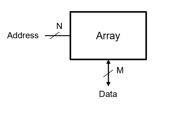
Fig. 2. Conceptual memory array: rows are addressable locations (depth = \(2^N\)), columns are the bit positions within each word (width = M).
At the physical level, this array is organized as a two-dimensional grid of bit cells — each cell storing exactly one bit (0 or 1). Rows represent addressable memory locations; columns represent the individual bit positions within each word.
Two parameters fully describe any memory array:
N address bits → selects one of \(2^N\) rows (the depth)
M data bits → the number of bits in each word (the width)
Memory Array Size
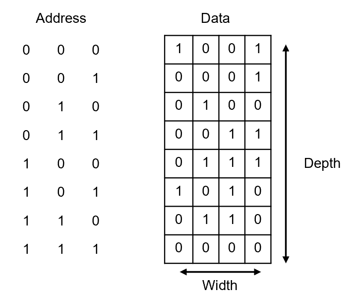
Fig. 3. Example memory array with binary addresses (left column) and stored data words (right column).
Wordlines and Bitlines#
Inside the array, two types of control signals access individual bit cells:
Wordline — a row-select signal. When driven HIGH, it activates all bit cells in that row, connecting them to the bitlines for reading or writing. When LOW, those cells are electrically isolated and their stored values are unchanged.
Bitline — carries the actual data. During a write, the bitline drives a voltage (HIGH = 1, LOW = 0) into the activated cell. During a read, the cell’s stored charge influences the bitline voltage, which a sense amplifier detects and interprets.
The rule is simple: the wordline controls access, the bitline carries information. Every modern memory technology — DRAM, SRAM, flash — is built on this same wordline/bitline structure.
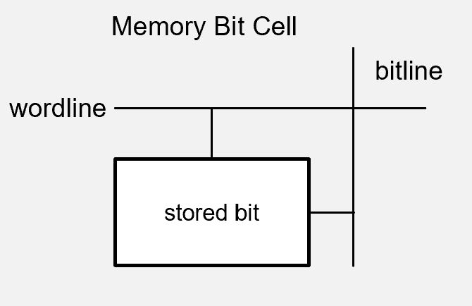
Fig. 4. Memory cell array showing wordline row-select connections and bitline data connections.
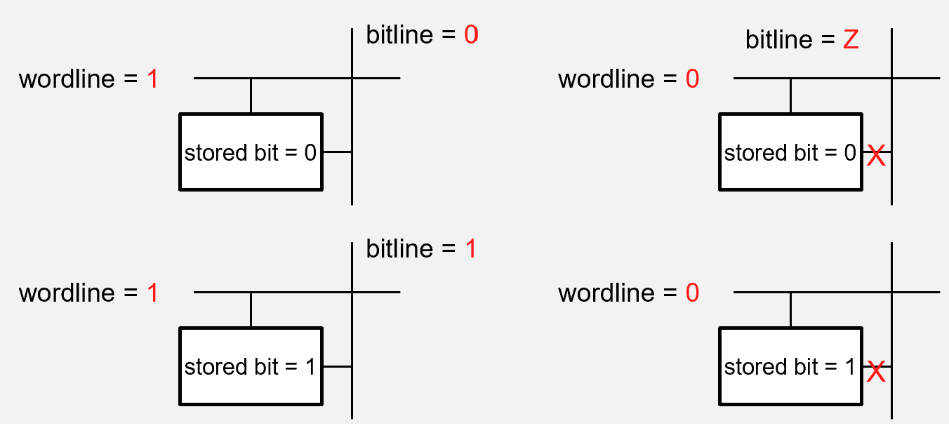
Fig. 5. Wordline and bitline signals during a read and write operation.
Example Problem 1 — Reading and Writing a Memory Array
Use the memory array shown below to answer: (a) At what address is the data 0100 stored? (b) What data is stored at address 101?
Fig. 6. Memory array used in Example Problem 1 — locate a given data word by address.
Understand: The address selects the row; the row contains the word. For part (a) we search the data column for the pattern. For part (b) we search the address column for the value.
Solve:
(a) Scanning the data column for 0100 — it appears in the row with address 010.
(b) Locating address 101 in the address column — its data entry reads 1010.
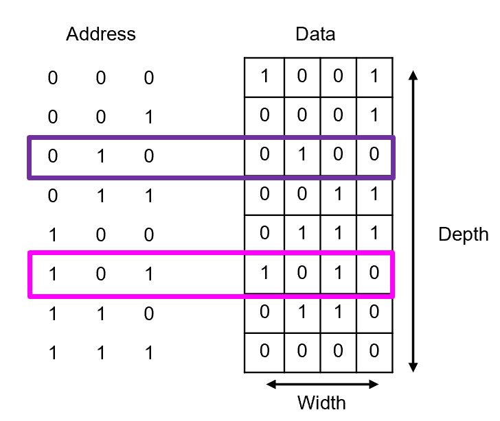
Fig. 7. Memory array with the accessed cells highlighted to show address-to-data mapping.
Answer: An address does not store data — it selects data. Each unique address maps to exactly one word. Every memory access follows the same rule: specify an address, get (or write) the word at that row.
Example Problem 2 — Sizing a Memory Array
(a) A memory is specified as “256-word × 16-bit.” How many address bits are required and what is the total storage capacity in bits?
(b) A memory array has 10 address bits and 8 data bits. What is its depth, width, and total size?
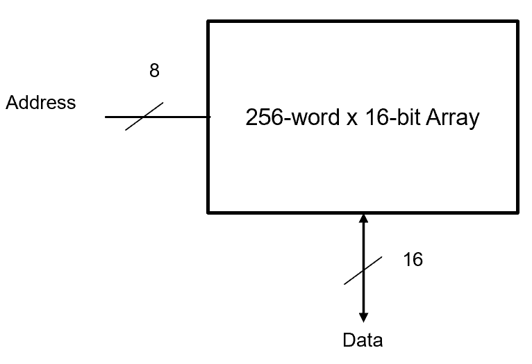
Fig. 8. Memory sizing diagram illustrating the 256-word × 16-bit specification.
Understand: Use Depth \(= 2^N\) to find the number of address bits when depth is given, and Total \(= 2^N \times M\) for capacity.
Solve:
(a) Depth = 256 words, Width = 16 bits.
(b) \(N = 10\), \(M = 8\).
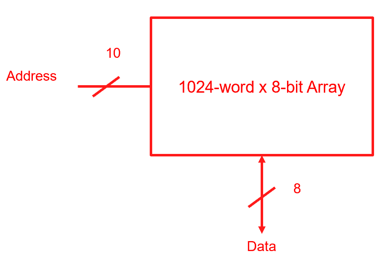
Fig. 9. Memory array illustrating the 1,024-word × 8-bit specification from part (b).
DRAM, SRAM, and ROM#
Not all memory is the same. The three main technologies differ in how they store bits, how fast they are, and whether they retain data when power is removed.
DRAM — Dynamic RAM#
DRAM is the dominant technology for main memory (the RAM in your laptop or desktop). It achieves high density and low cost by storing each bit in a 1T1C cell: one transistor and one capacitor.

Fig. 10. DRAM 1T1C cell: one access transistor controlled by the wordline and one capacitor storing the bit.
The capacitor stores charge to represent a 1 (charged) or 0 (discharged). The transistor, controlled by the wordline, acts as the access switch. The “dynamic” in DRAM refers to the fact that the stored charge leaks away over time — so every cell must be refreshed (rewritten) approximately every 64 milliseconds, or the data is lost.
DRAM also has a destructive read: accessing a cell redistributes its charge onto the bitline, partially draining the capacitor. The memory controller must therefore rewrite the original value after every read operation.
Write: Wordline goes HIGH → transistor turns ON → bitline voltage charges or discharges the capacitor → wordline goes LOW, trapping the stored value.
Read: Wordline goes HIGH → stored charge redistributes onto the bitline → sense amplifier detects the tiny voltage change → value is interpreted and then rewritten into the cell.
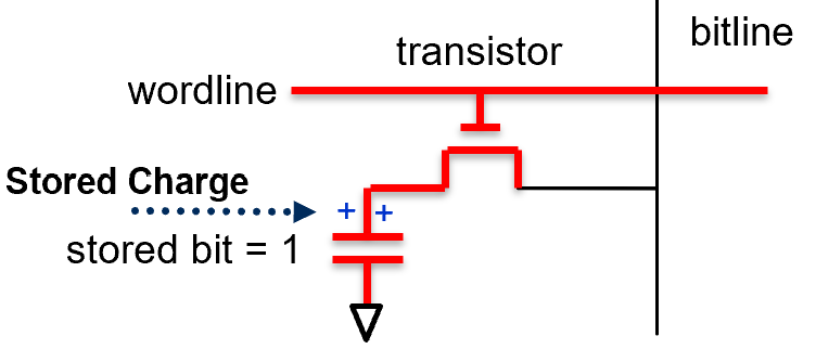
Fig. 11. DRAM read and write sequence: wordline pulse enables the transistor; the bitline charges or discharges the storage capacitor.
SRAM, ROM, and the Comparison#
SRAM (Static RAM) stores each bit in a cross-coupled inverter circuit (typically 6 transistors). It holds its state as long as power is applied, requires no refresh, and is significantly faster than DRAM — which is why processors use it for cache. The tradeoff is cost and density: SRAM cells are much larger than 1T1C DRAM cells.
ROM (Read-Only Memory) is non-volatile — it retains data without power. It holds firmware, BIOS, and other fixed instructions that must survive power cycles.
Feature |
DRAM |
SRAM |
ROM |
|---|---|---|---|
Volatility |
Volatile |
Volatile |
Non-volatile |
Refresh needed |
Yes |
No |
N/A |
Speed |
Moderate |
Very fast |
Slow |
Cell design |
1T1C |
6 transistors |
Fixed |
Density |
High |
Low |
Varies |
Primary use |
Main memory |
Processor cache |
Firmware, BIOS |
Assembly Language and Machine Code#
The CPU only understands binary — sequences of 0s and 1s that encode both instructions and data. Two layers of abstraction sit between the programmer and the hardware.
Machine code is the native language of the processor: raw binary patterns where some bits specify the operation (the opcode), others specify registers, and others specify memory addresses. Because long binary strings are unreadable, machine code is often represented in hexadecimal, where each hex digit represents 4 bits.
Assembly language provides a human-readable shorthand for the same instructions. Instead of writing 10110010 00000101, you write ADD 5. An assembler translates these mnemonics back into binary before the processor executes them. Assembly is architecture-specific — code written for an Intel x86 processor cannot run directly on an ARM processor because the instruction sets are different.
Instruction |
Description |
|---|---|
|
Load the value at address X into the accumulator |
|
Store the accumulator’s value into address X |
|
Add the value at address X to the accumulator |
|
Subtract the value at address X from the accumulator |
|
Multiply the value at address X by the accumulator |
|
Divide the accumulator by the value at address X |
|
Compare the value at address X to the value at address Y |
|
Jump to address Z if the last comparison result was greater than |
|
Jump to address Z if the last comparison result was less than or equal |
Inside the CPU, three registers are central to instruction execution:
Program Counter (PC) — holds the address of the next instruction to fetch. After each fetch, PC increments by 1. A jump instruction sets PC to a new address.
Instruction Register (IR) — holds the instruction currently being decoded and executed.
Accumulator — the working register for arithmetic and logical results. Most operations implicitly use it.
The Fetch–Decode–Execute Cycle#
Every instruction the CPU executes follows the same three-step rhythm:
Fetch — read the instruction at address PC into the IR; increment PC
Decode — the Control Unit examines the IR to determine what operation to perform and what operands to use
Execute — carry out the operation: compute, move data, or update PC for a branch
This cycle repeats billions of times per second. Every program — from a simple addition to a flight control algorithm — is nothing more than this loop running on a stream of binary instructions.
Example Problem 3 — Fetch–Decode–Execute: Adding Two Numbers
Trace the fetch–decode–execute cycle for the program below. What is the final state of memory?
Initial RAM:
Address |
Value |
|---|---|
0 |
LOAD 4 |
1 |
ADD 5 |
2 |
STORE 6 |
3 |
0 |
4 |
2 |
5 |
7 |
6 |
0 |
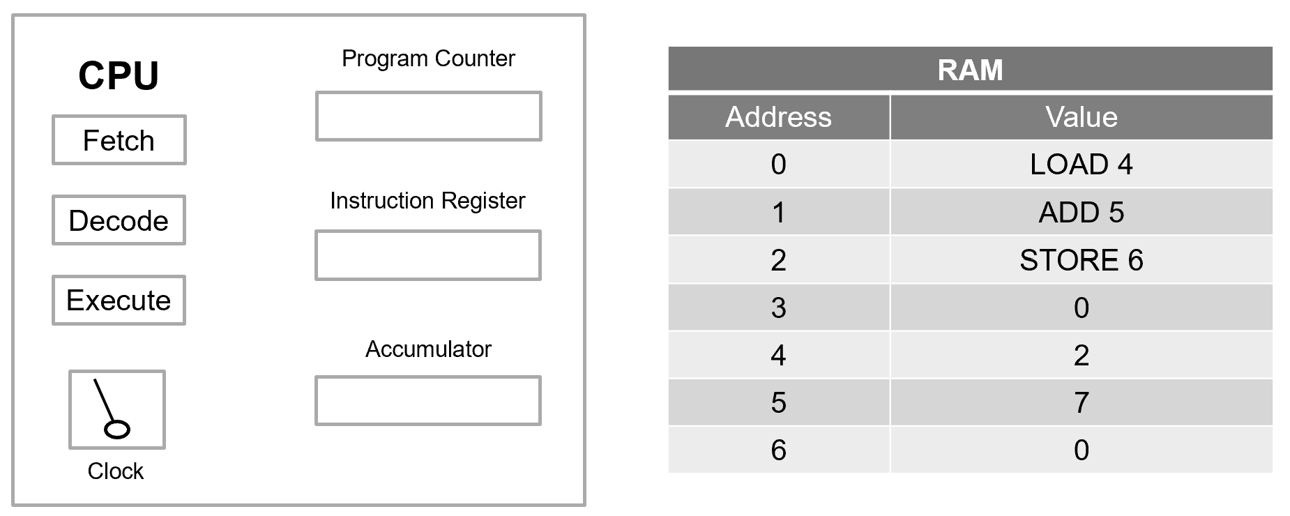
Fig. 12. Initial RAM state for Example Problem 3: instructions at addresses 0–2, data values at addresses 4–6.
Understand: Addresses 0–2 are instructions; addresses 3–6 are data. The PC starts at 0. Trace each instruction through fetch → decode → execute.
Solve:
Cycle 1 — Instruction at address 0: LOAD 4
Fetch: IR ←
LOAD 4; PC ← 1Decode: load the value at address 4 into the accumulator
Execute: Accumulator ← Memory[4] = 2
Cycle 2 — Instruction at address 1: ADD 5
Fetch: IR ←
ADD 5; PC ← 2Decode: add the value at address 5 to the accumulator
Execute: Accumulator ← 2 + Memory[5] = 2 + 7 = 9
Cycle 3 — Instruction at address 2: STORE 6
Fetch: IR ←
STORE 6; PC ← 3Decode: write the accumulator’s value to address 6
Execute: Memory[6] ← 9
Final RAM state:
Address |
Value |
|---|---|
0 |
LOAD 4 |
1 |
ADD 5 |
2 |
STORE 6 |
3 |
0 |
4 |
2 |
5 |
7 |
6 |
9 |
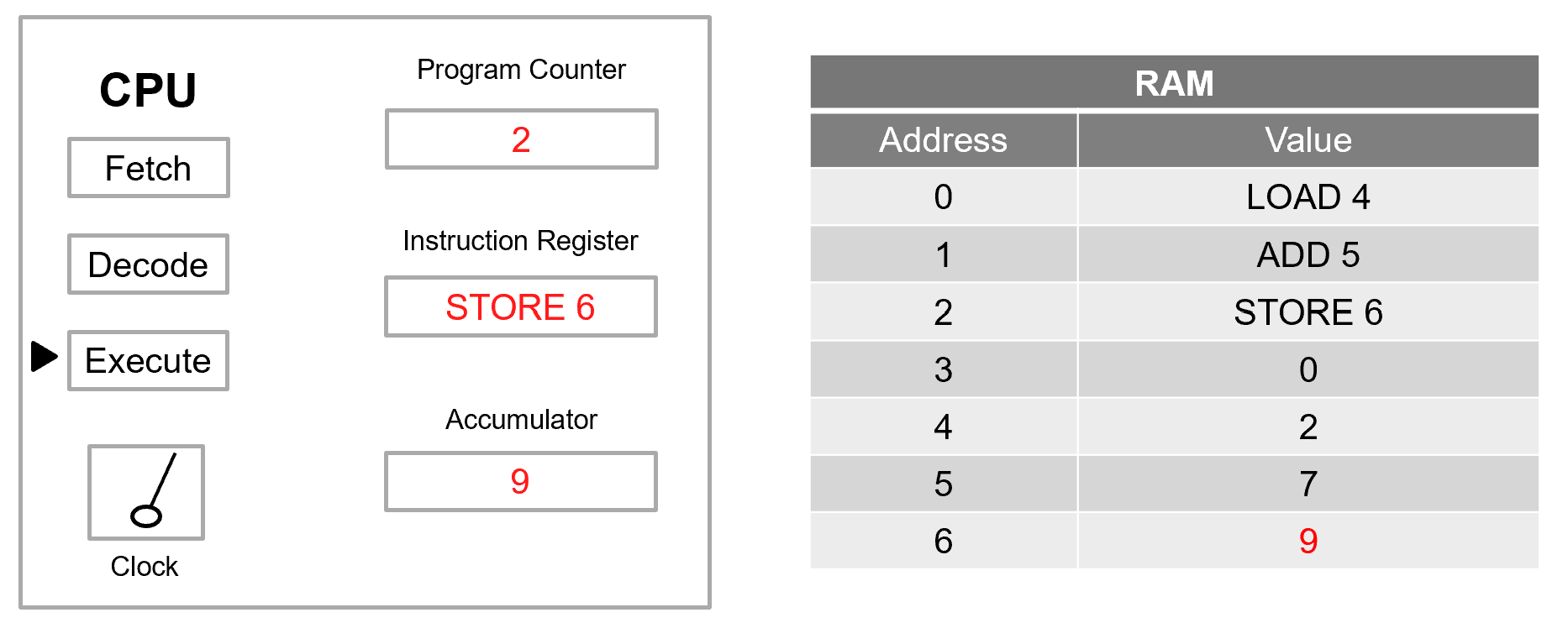
Fig. 13. Final RAM state for Example Problem 3: address 6 now holds 9 after the STORE instruction executes.
Answer: The result 9 is stored at address 6. Notice that memory only changes when a STORE instruction executes — all arithmetic happens inside the processor, and the result stays in the accumulator until explicitly written back.
Example Problem 4 — Branching and Conditional Jumps
Trace execution of the program below. Where does the Program Counter end up?
Initial RAM:
Address |
Value |
|---|---|
0 |
LOAD 7 |
1 |
ADD 8 |
2 |
STORE 9 |
3 |
CMP 9, 10 |
4 |
JG 6 |
5 |
JLE 0 |
6 |
NEXT_SW_ACTION |
7 |
5 |
8 |
6 |
9 |
0 |
10 |
7 |
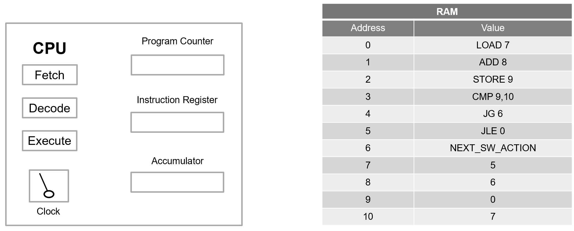
Fig. 14. Initial RAM state for Example Problem 4: arithmetic instructions at 0–2, comparison and branch instructions at 3–5, data at 7–10.
Understand: This program adds two values, stores the result, then compares it against a threshold. Depending on the outcome, execution either continues forward or jumps back to the start.
Solve:
LOAD 7: Accumulator ← Memory[7] = 5
ADD 8: Accumulator ← 5 + Memory[8] = 5 + 6 = 11
STORE 9: Memory[9] ← 11
CMP 9, 10: Compare Memory[9] = 11 against Memory[10] = 7. The processor subtracts internally: \(11 - 7 > 0\), so the greater-than flag is set. The accumulator is unchanged.
JG 6: The greater-than condition is true → PC ← 6
The instruction at address 5 (JLE 0) is skipped. Execution continues at address 6.
Answer: PC = 6. The comparison does not modify data — it sets internal status flags. The branch instruction then reads those flags to decide whether to redirect execution. Without branching, programs could only run in a straight line. Conditional jumps are what enable if/else logic, loops, and any form of decision-making.
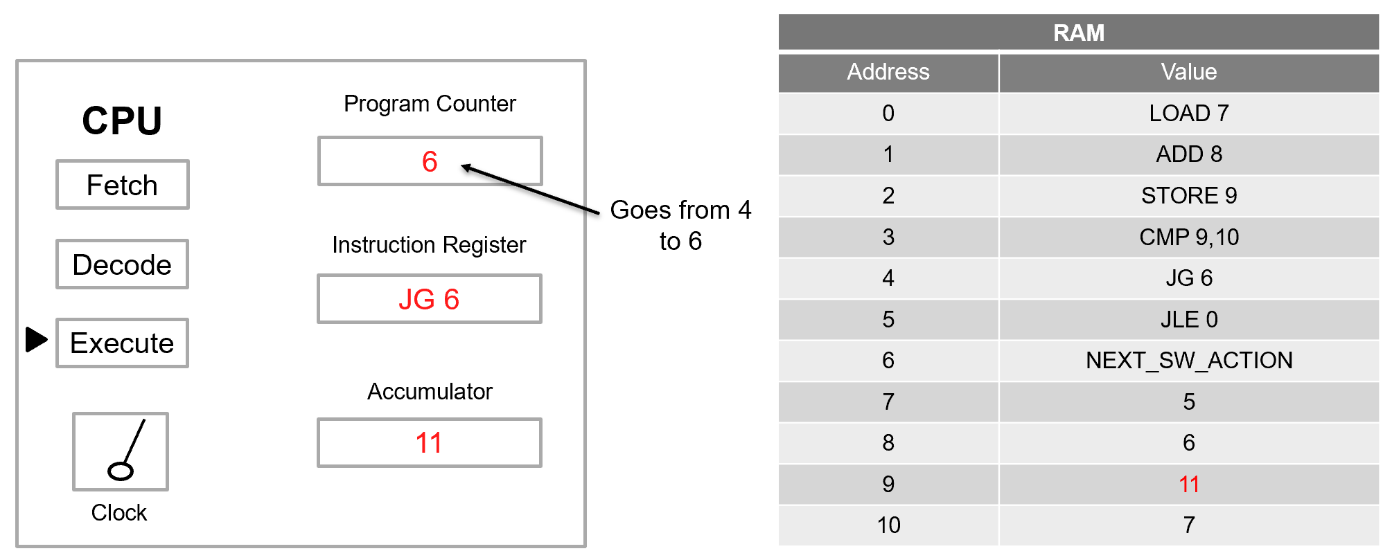
Fig. 15. Program Counter after branching in Example Problem 4 — JG condition is true, so PC jumps to address 6.
Example Problem 5 — Infinite Loop
The program from Example Problem 4 runs again, but address 8 now holds 1 instead of 6. What happens?
Address |
Value |
|---|---|
0 |
LOAD 7 |
1 |
ADD 8 |
2 |
STORE 9 |
3 |
CMP 9, 10 |
4 |
JG 6 |
5 |
JLE 0 |
6 |
NEXT_SW_ACTION |
7 |
5 |
8 |
1 |
9 |
6 |
10 |
7 |
Understand: The only change is Memory[8] = 1 instead of 6. Trace the arithmetic and comparison to see how branching changes.
Solve:
LOAD 7: Accumulator ← 5
ADD 8: Accumulator ← 5 + 1 = 6
STORE 9: Memory[9] ← 6
CMP 9, 10: Compare 6 against 7. Since \(6 \leq 7\), the less-than-or-equal flag is set.
JG 6: Condition is false — do not jump.
JLE 0: Condition is true → PC ← 0
Execution returns to address 0. The arithmetic runs again: \(5 + 1 = 6\), \(6 \leq 7\), jump back to 0… forever.
Answer: The program is stuck in an infinite loop. Because no instruction ever modifies the values at addresses 7, 8, or 10, the comparison outcome never changes, and the branch always redirects back to the start. This is the hardware-level origin of the “infinite loop” bug — a comparison that can never change its result, combined with a branch that always triggers.
Key Takeaways#
Von Neumann Architecture. The foundational computer design model in which instructions and data are stored together in the same physical memory and shared communication pathways, making general-purpose computing possible.
Stored-program concept. Programs are treated as data in memory, so changing what a computer does requires only loading different data rather than physically rewiring the hardware.
Memory array organization. Memory is a 2D grid of bit cells addressed by \(N\) address bits (giving \(2^N\) rows of depth) and \(M\) data bits wide, with total capacity \(= 2^N \times M\) bits.
DRAM vs. SRAM. DRAM stores each bit in a 1-transistor/1-capacitor cell (high density, requires periodic refresh) while SRAM uses a 6-transistor cross-coupled inverter (faster and no refresh needed, but lower density); SRAM is used for processor cache, DRAM for main memory.
ROM. Read-Only Memory is non-volatile — it retains data without power — making it suitable for firmware and BIOS that must survive power cycles.
Fetch-Decode-Execute cycle. Every instruction follows a three-step rhythm: the CPU fetches the instruction at the address in the Program Counter, decodes its meaning, then executes the operation and increments the PC.
Accumulator and registers. The accumulator holds the working result of arithmetic operations inside the CPU; memory only changes when an explicit STORE instruction writes the accumulator’s value back to a RAM address.
Conditional branching. Jump instructions read internal status flags set by compare operations and redirect the Program Counter to a new address, enabling loops, if/else decisions, and all higher-level program control flow.